Manufacturing method for self-protection silicon-based APD array device with temperature compensation

An APD array, temperature compensation technology, used in semiconductor/solid-state device manufacturing, electrical components, circuits, etc., can solve the problem of being unable to cope with the requirements of weak optical signal detection, and achieve the effect of reducing multiplication noise

Inactive Publication Date: 2016-01-27
哈尔滨伽马光电科技有限公司
View PDF3 Cites 3 Cited by
  • Summary
  • Abstract
  • Description
  • Claims
  • Application Information

AI Technical Summary

Problems solved by technology

However, the carrier does not have a multiplication process inside the PIN photodiode device. For a single photon, only a pair of electron-hole pairs can be generated, which cannot meet the requirements of weak optical signal detection.

Method used


Image

  • Manufacturing method for self-protection silicon-based APD array device with temperature compensation
  • Manufacturing method for self-protection silicon-based APD array device with temperature compensation
  • Manufacturing method for self-protection silicon-based APD array device with temperature compensation

Examples


Embodiment Construction

[0014] The core idea of ​​the present invention is to provide a method for manufacturing a silicon-based APD array device with temperature compensation and self-protection.

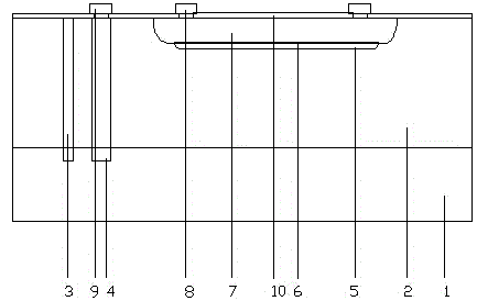
[0015] Below in conjunction with the specific implementation and image 3 The present invention will be further described. The advantages and features of the present invention will be apparent from the following description and claims. It should be noted that all the drawings are in a very simplified form and use imprecise scales, and are only used to facilitate and clearly assist the purpose of illustrating the embodiments of the present invention.

[0016] First, a silicon wafer is provided as a substrate 1, and the substrate is a P-type silicon wafer doped with boron.

[0017] Secondly, epitaxial growth is performed on the substrate 1 to form an epitaxial layer as the absorption region 2 of the device, and the epitaxial layer is doped with boron.

[0018] Next, oxide layer deposition, photolithograp...


PUM


Abstract

The invention relates to a manufacturing method for a self-protection silicon-based APD array device with temperature compensation. The structure of the self-protection silicon-based APD array device comprises an avalanche photodiode (APD) array, a temperature-sensitive diode and a quenching resistor, wherein the avalanche photodiode (APD) array is composed of micro-unit APDs, the quenching resistor is connected with each micro-unit APD in series to form a unit, all the units are connected in parallel to form a linear array, and the linear array device is connected with the temperature-sensitive diode in a surface mounting manner. The APD array of the structure has the advantages of good temperature compensatory, high uniformity, fast response speed, low noise and the like.

Description

technical field [0001] The invention relates to the field of optoelectronic device manufacturing, in particular to a manufacturing method of a silicon-based APD array device with temperature compensation and self-protection. Background technique [0002] There are mainly two types of photodetectors currently used, namely PIN photodiodes and APD photodiodes. Due to the advantages of simple manufacturing process and low cost, PIN photodiodes are widely used in optical fiber communication. However, there is no multiplication process of carriers in the PIN photodiode device, and only a pair of electron-hole pairs can be generated for a single photon, which cannot meet the requirements of weak optical signal detection. After the APD photodiode absorbs photons, it will generate electron-hole pairs in the space charge region. Under the action of a strong electric field, the carriers in the semiconductor will undergo an avalanche multiplication effect, and the received single photo...

Claims


Application Information

Patent Timeline
Patent Type & Authority Applications(China)
IPC IPC(8): H01L21/77
Inventor 不公告发明人
Owner 哈尔滨伽马光电科技有限公司
Why Eureka
Try Eureka