
A circuit board 3D printing method with spatial three-dimensional circuit

A space three-dimensional, 3D printing technology, applied in the field of 3D printing, can solve the problems of shape structure design limitation, circuit board space occupation, high cost of composite process, achieve fast forming speed, optimize shape structure, and solve the effect of low space utilization rate

Active Publication Date: 2018-02-23
HUAZHONG UNIV OF SCI & TECH
View PDF6 Cites 0 Cited by
  • Summary
  • Abstract
  • Description
  • Claims
  • Application Information

AI Technical Summary

Problems solved by technology

However, both of the above two circuit board manufacturing schemes use two different 3D printing processes to form a conventional circuit board with a single flat structure. The circuit board still occupies a considerable part of the space in electronic equipment, and the heat dissipation is too concentrated; on the other hand, the shape and structure design of the equipment is still limited, and the advantages of 3D printing for structural free design are greatly restricted

Method used


Image

  • A circuit board 3D printing method with spatial three-dimensional circuit
  • A circuit board 3D printing method with spatial three-dimensional circuit

Examples


Embodiment 1

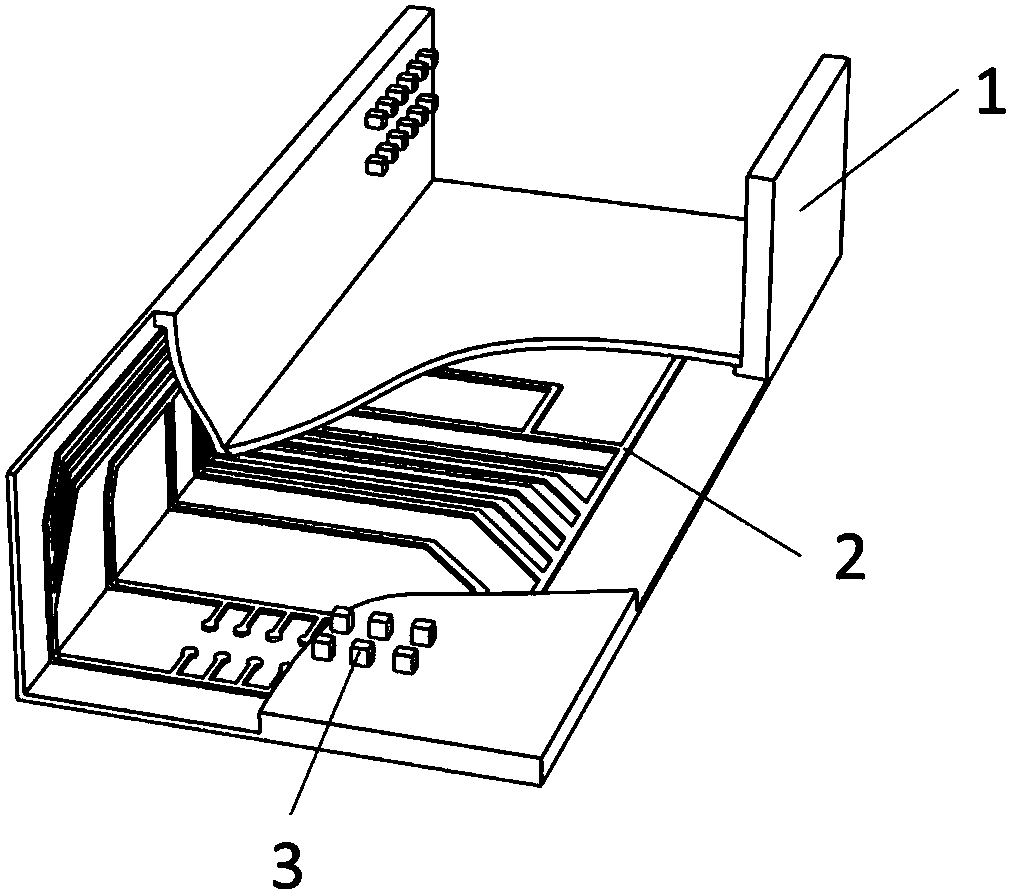
[0036] 1) Use 3D modeling software to design such as figure 1 The structural model of the cuboid-shaped part product (belonging to the circuit board) shown, and the circuit lines distributed with the structural shape, wherein 1 is the product structure part, 2 is the circuit line part, and 3 is the interface for chip insertion;

[0037] 2) Using slicing software to slice the model layer by layer, each layer thickness is 0.1mm, and identify the product structure part 1 and the circuit circuit part 2 in each layer in the slicing information;

[0038] 3) Input the structural information and circuit line information identified by each layer to the FDM terminal equipped with dual nozzles. The dual nozzles (built-in heating rod brass nozzles, nozzle diameter range 0.2mm-0.4mm) include front nozzles and rear nozzles The work is controlled by the control system. The material in the feeding system of the front nozzle is ABS wire with a diameter of 1.8mm; the feeding system of the rear ...

Embodiment 2

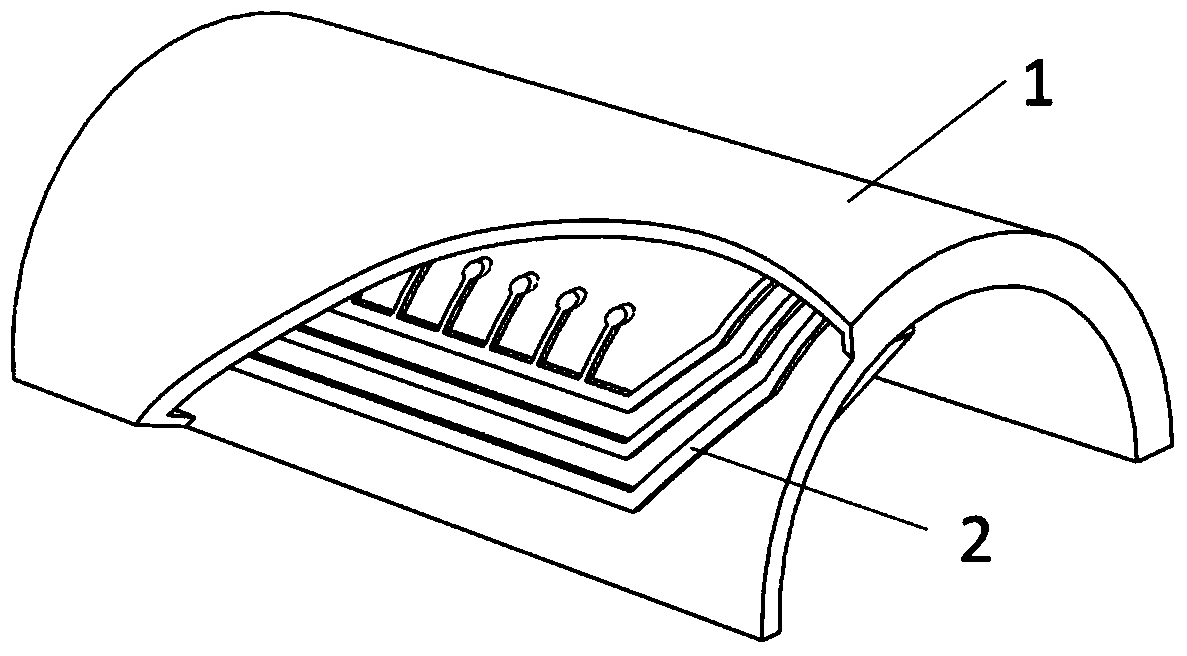
[0042] 1) Use 3D modeling software to design such as figure 2 The structural model of the semi-cylindrical part product (belonging to the circuit board) shown, and the circuit lines distributed with the structural shape, wherein 1 is the structural part of the model, and 2 is the circuit line part;

[0043] 2) Using slicing software to slice the model layer by layer, each layer thickness is 0.1mm, and identify the product structure part 1 and the circuit circuit part 2 in each layer in the slicing information;

[0044] 3) Input the structural information and circuit line information identified by each layer to the FDM terminal equipped with dual nozzles. The dual nozzles (built-in heating rod brass nozzles, nozzle diameter range 0.2mm-0.4mm) are divided into front nozzles and rear nozzles. The nozzle is controlled by the control system. The material in the feeding system of the front nozzle is nylon wire with a diameter of 1.6mm; the feeding system of the rear nozzle is silve...


PUM


Abstract

The invention discloses a 3D printing method for a circuit board with a space three-dimensional circuit. The 3D printing method comprises the following steps that a circuit board structure model and a circuit line are designed by utilizing three-dimensional modeling software; the circuit board structure model is hierarchically sliced by utilizing slicing software, and structure and circuit line information in slicing layers is identified; identification information of each layer is inputted to FDM equipment equipped with double nozzles; deposition and formation are performed layer by layer by the double nozzles according to the structure information and the circuit line information of each layer, a formed piece is enabled to drop a height of preset layer thickness when deposition and formation of one slicing layer are completed in the formation process, the next slicing layer is deposited on the formed slicing layer by the double nozzles continuously, and circulating stacking is performed layer by layer until printing of the whole circuit board is completed; and post-processing is performed on the circuit board so that the required circuit board is obtained. According to the method, the conventional manufacturing process is greatly simplified, the manufacturing period is shortened, manufacturing cost is reduced and degree of freedom of electronic product appearance structure design can be substantially enhanced.

Description

technical field [0001] The invention belongs to the technical field of 3D printing, and more specifically relates to a 3D printing method for a circuit board with a spatial three-dimensional circuit. Background technique [0002] The electronic product system is composed of parts, components, etc. In its manufacturing process, the parts and components are first assembled into components, and then the components are assembled into a complete machine. The core work is to assemble the components into circuits with certain functions Board components, therefore, the core of electronic product manufacturing lies in the manufacture of printed circuit boards (Printed Circuit Board, PCB). The circuit board is the carrier of the electrical connection of electronic components. Almost every kind of equipment with integrated circuit electronic components, such as watches, calculators, computers, communication equipment, etc., must use printed circuit boards, so the design and manufacture...

Claims


Application Information

Patent Timeline
Patent Type & Authority Patents(China)
IPC IPC(8): H05K3/00H05K3/14
CPCH05K3/0011H05K3/14H05K2203/0126
Inventor 魏青松韩昌骏谭杰文刘洁史玉升
Owner HUAZHONG UNIV OF SCI & TECH
Learn More