Low temperature polycrystalline silicon thin film transistor and manufacturing method therefor

A technology of thin-film transistors and low-temperature polysilicon, which is applied in the direction of transistors, semiconductor/solid-state device manufacturing, semiconductor devices, etc., and can solve problems such as small contact area, large contact resistance, and polysilicon film loss

Inactive Publication Date: 2016-02-10
WUHAN CHINA STAR OPTOELECTRONICS TECH CO LTD
View PDF3 Cites 8 Cited by
  • Summary
  • Abstract
  • Description
  • Claims
  • Application Information

AI Technical Summary

Problems solved by technology

The etching process of the interlayer dielectric layer 110 will directly etch to the polysilicon film layer, resulting in the loss of the polysilicon film; at the same time, the bottom area of ​​the via hole 114 of the interlayer dielectric layer 110 and the polysilicon film are in metal contact with the source electrode/drain electrode 112 The area is small, and the metal contact resistanc

Method used


Image

  • Low temperature polycrystalline silicon thin film transistor and manufacturing method therefor
  • Low temperature polycrystalline silicon thin film transistor and manufacturing method therefor
  • Low temperature polycrystalline silicon thin film transistor and manufacturing method therefor

Examples


Embodiment Construction

[0030] The description of the present invention provides different examples to illustrate the technical features of different implementations of the present invention. The configuration of each component in the embodiment is for clearly illustrating the content disclosed in the present invention, and is not intended to limit the present invention. In different drawings, the same reference symbols refer to the same or similar components.

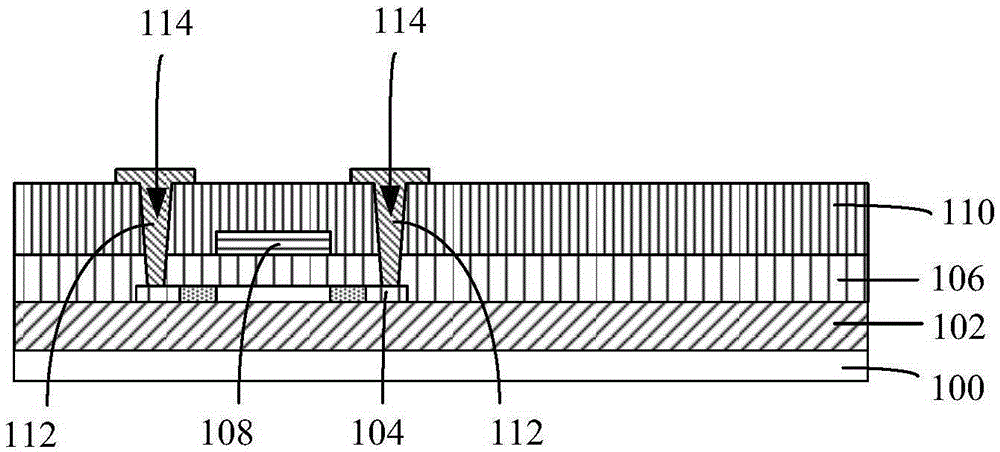
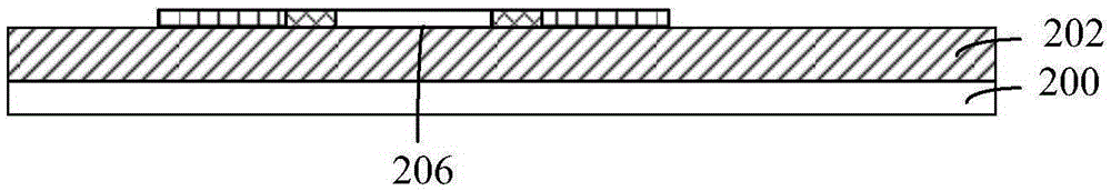
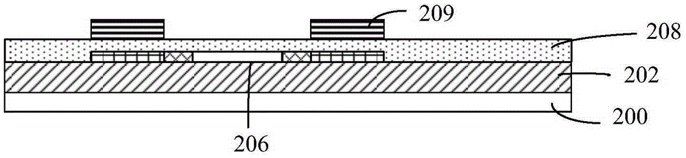
[0031] refer to Figure 2-8 , Figure 2-8 It is a schematic cross-sectional view of the manufacturing process steps of a low-temperature polysilicon thin film transistor according to an embodiment of the present invention. Such as figure 2 As shown, a substrate 200 is provided. In one embodiment, the substrate 200 is, for example, a glass substrate, a quartz substrate, a stainless steel substrate or a plastic substrate.

[0032] Such as figure 2 As shown, a buffer layer 202 is formed on the substrate 200 . In one embodiment, the buff...


PUM

PropertyMeasurementUnit
Thicknessaaaaaaaaaa

Abstract

The invention relates to a low temperature polycrystalline silicon thin film transistor and a manufacturing method therefor. A conductive buffer cushion is arranged in a source electrode region and a drain electrode region for preventing the polycrystalline silicon in a contact hole from being etched; and the electrical conductivity among the polycrystalline silicon layer, the source electrode and the drain electrode is improved so as to reduce contact resistance and improve the assembly performance of the polycrystalline silicon thin film transistor.

Description

【Technical field】 [0001] The invention relates to a manufacturing method of a thin film transistor, and in particular to a low-temperature polysilicon thin film transistor and a manufacturing method thereof. 【Background technique】 [0002] With the development of semiconductor technology, video products, especially digital video or image devices have become common products in daily life. In these digital video or image devices, the display is an important component to display relevant information. Low-temperature polysilicon thin-film transistors (LTPSTFT) can be applied to the driving components of liquid crystal displays, making this product the mainstream of displays, and will become a future dominant product in markets such as personal computers, game consoles, and monitors. [0003] In the process structure of low-temperature polysilicon thin-film transistor (LTPSTFT) liquid crystal display panel, during the production process of inter-layer dielectric layer (inter-lay...

Claims


Application Information

Patent Timeline
IPC IPC(8): H01L21/336H01L29/786H01L29/06
CPCH01L29/66757H01L29/06H01L29/0603H01L29/78672H01L29/78675
Inventor 张占东
Owner WUHAN CHINA STAR OPTOELECTRONICS TECH CO LTD
Why Eureka
Try Eureka