Packaging method of OLED (organic light emitting diode) display panel

A display panel and packaging method technology, which is applied in the direction of organic light-emitting devices, semiconductor devices, electrical components, etc., can solve the problems of lower production efficiency of OLED display panels, lower paste efficiency of external barrier films, and lead wires in easily damaged binding areas. Achieve the effects of improving life and safety, improving paste efficiency, and improving paste efficiency

Active Publication Date: 2016-02-10
KUNSHAN NEW FLAT PANEL DISPLAY TECH CENT +1
View PDF4 Cites 29 Cited by
  • Summary
  • Abstract
  • Description
  • Claims
  • Application Information

AI Technical Summary

Problems solved by technology

The disadvantage of this approach is that in addition to the effective display area of ​​the OLED display panel, the binding area will also be covered by the outer barrier film. area-specific leads
[0005] However, the above two methods will reduce the paste efficiency of the external barrier film, thereby causing a decline in the overall production efficiency of the OLED display panel; and pasting one by one or in a small area will affect the paste accuracy of the external barrier film, and it is easy to cause distorted pasting. Phenomenon, affecting the pass rate of the product

Method used


Image

  • Packaging method of OLED (organic light emitting diode) display panel
  • Packaging method of OLED (organic light emitting diode) display panel
  • Packaging method of OLED (organic light emitting diode) display panel

Examples


preparation example Construction

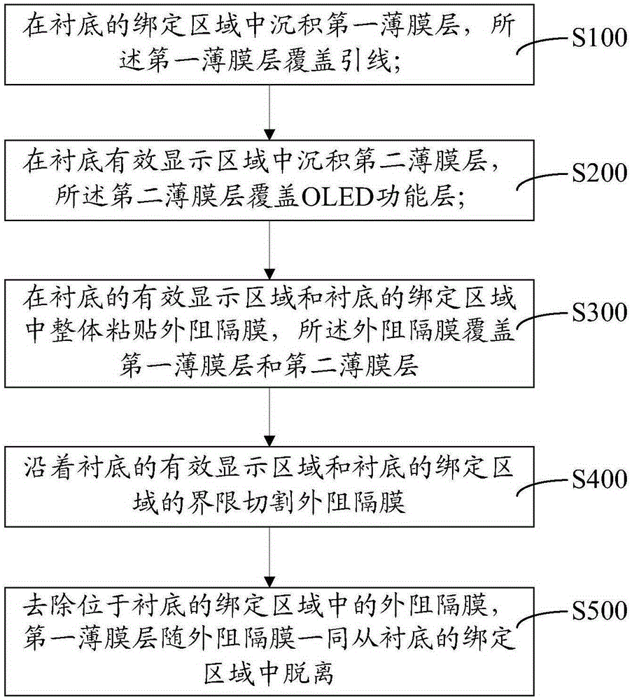
[0039] During the preparation of the OLED functional layer 200, a mask is usually used to cover the binding region 120 of the substrate 100, and then a thin film transistor, an anode electrode layer, an organic material layer, Cathode electrode layer and light coupling layer. Preferably, when depositing an organic material layer or an optical coupling layer in the effective display area 110, the first thin film layer 400 can be deposited in the binding area 120 at the same time, which can be specifically implemented in the following manner: depositing an organic material layer in the effective display area 110 material layer or optical coupling layer, the position corresponding to the binding region 120 of the substrate 100 in the mask is designed as a hollow structure, so that the organic material layer or optical coupling layer can be simultaneously deposited on the effective display of the substrate 100 In the area 110 and the binding area 120, the organic material layer or...

Embodiment 1

[0064] (1) When the hole injection layer is evaporated in the effective display area 110 of the substrate 100, the hole injection layer is evaporated in the binding area 120 of the substrate 100 at the same time, and the holes deposited in the binding area 120 The injection layer serves as the first film layer 400;

[0065] (2) Depositing the second thin film layer 300 on the surface of the OLED functional layer 200 located in the effective display area 110 by alternately depositing organic materials and inorganic materials;

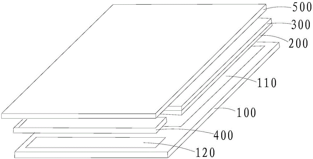
[0066] (3) paste one deck outer barrier film 500 on the surface of the first film layer 400 and the second film layer 300 as a whole;

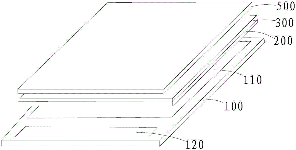
[0067] (4) cutting the outer barrier film 500 along the boundary between the binding area 120 and the effective display area 110 by laser cutting;

[0068] (5) Tear off the outer barrier film 500 located in the binding area 120, and the first film layer 400 is adhered under the sticking force of the outer barrier film 5...

Embodiment 2

[0071] (1) When the optical coupling layer is evaporated on the effective display area 110 of the substrate 100, the optical coupling layer is evaporated in the binding area 120 of the substrate 100 at the same time, and the optical coupling layer evaporated in the binding area 120 as the first film layer 400;

[0072] (2) Depositing the second thin film layer 300 on the surface of the OLED functional layer 200 located in the effective display area 110 by alternately depositing organic materials and inorganic materials;

[0073] (3) paste one deck outer barrier film 500 on the surface of the first film layer 400 and the second film layer 300 as a whole;

[0074] (4) The substrate 100 of the OLED display panel is integrally peeled off from the glass substrate by laser peeling, and then the OLED display panel obtained after peeling is cut into several small screen bodies according to the process requirements;

[0075] (5) Cutting the outer barrier film 500 along the boundary betw...


PUM


Abstract

The invention discloses a packaging method of an OLED (organic light emitting diode) display panel. The method comprises the following steps: depositing a first film layer in a binding area of a substrate, wherein the first film layer covers a lead; depositing a second film layer in an effective display area of the substrate, wherein the second film layer covers an OLED functional layer; integrally adhering an outer obstruction film in the effective display area of the substrate and the binding area of the substrate, wherein the outer obstruction film covers the first film layer and the second film layer; cutting the outer obstruction film along a boundary of the effective display area and the binding area of the substrate; and removing the outer obstruction film in the binding area of the substrate, wherein the first film layer is separated from the effectively display area along with the obstruction film. The outer obstruction film is adhered in an integral pasting manner, so that the adhesion efficiency and adhesion precision of the outer obstruction film are effectively improved, damage on the lead in the binding area during the separation process of the outer obstruction film is avoided, the service life of the OLED display panel is prolonged, and the application safety is improved.

Description

technical field [0001] The invention relates to the field of display technology, in particular to a packaging method for an OLED display panel. Background technique [0002] The packaging of OLED (Organic Light-Emitting Diode, Organic Light-Emitting Diode) display panel is mainly to isolate the OLED from the external environment to prevent the intrusion of moisture, oxidizing gas, dust rays and external force damage, thereby stabilizing the parameters of the device and improving the service life . [0003] At present, the packaging of flexible OLED display panels mostly adopts thin-film packaging technology. Generally, a barrier layer is deposited on the surface of the effective display area of ​​the OLED display panel to avoid contact between the OLED and the external environment. In order to achieve a better isolation effect, an outer barrier film is usually pasted on the outer surface of the barrier layer to achieve double isolation. The traditional method is to paste a...

Claims


Application Information

Patent Timeline
Patent Type & Authority Applications(China)
IPC IPC(8): H01L51/56H01L51/52H01L27/32
CPCH10K59/00H10K50/844H10K50/8445H10K71/00
Inventor 赵长征罗志忠周斯然刘金强敖伟
Owner KUNSHAN NEW FLAT PANEL DISPLAY TECH CENT
Why Eureka
Try Eureka