Control device and method for achieving wide-range scanning of electron beam and additive manufacturing device

A control device and electron beam technology, which is applied in the field of additive manufacturing, can solve the problems of small defocus and astigmatism, small deflection angle, and inability to realize wide-width scanning of electron beams, achieving high-quality scanning, strong operability, The effect of improving the molding quality

Inactive Publication Date: 2016-02-17
QUICKBEAM CO LTD +1
View PDF6 Cites 29 Cited by
  • Summary
  • Abstract
  • Description
  • Claims
  • Application Information

AI Technical Summary

Problems solved by technology

[0009] The current problem is that in electron beam processing technologies such as electron beam welding and electron beam melting, the deflection angle of the electron beam is small, and the defocus and astigmatism caused by the large deflection of the electron beam are relatively small, which will not affect welding or melting. quality
Therefore, in this kind of electron beam processing equipment, there are generally only focusing coils and deflection coils, so high-precision wide-width scanning of the electron beam cannot be realized.
[0010] At the same time, the existing electron beam selective melting additive manufacturing equipment generally uses electron beam generating devices for electron beam welding, which also cannot achieve high-precision wide-width scanning of electron beams.

Method used


Image

  • Control device and method for achieving wide-range scanning of electron beam and additive manufacturing device
  • Control device and method for achieving wide-range scanning of electron beam and additive manufacturing device
  • Control device and method for achieving wide-range scanning of electron beam and additive manufacturing device

Examples


Embodiment Construction

[0053] In order to make the object, technical solution and advantages of the present invention clearer, the present invention will be described in further detail below in conjunction with specific embodiments and with reference to the accompanying drawings.

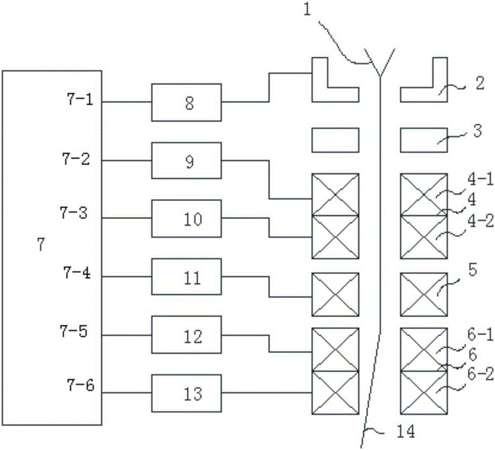
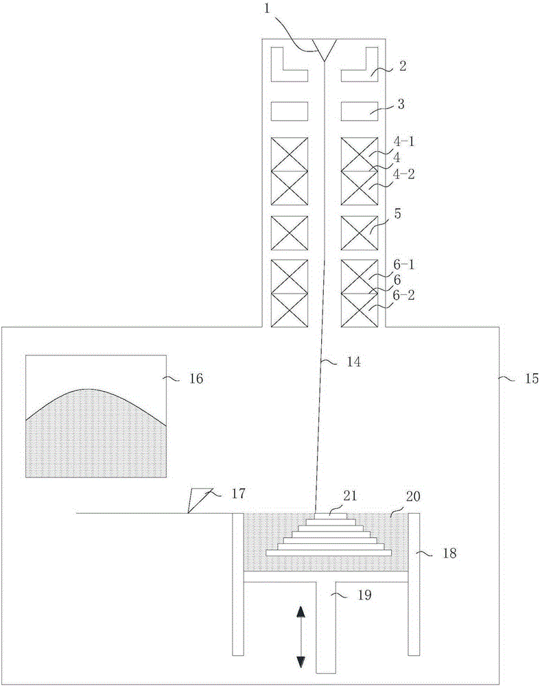
[0054] figure 1 It is a schematic diagram of the control device for electron beam wide scanning according to the present invention.

[0055] Electrons are generated from cathode 1 and pass through grid 2 , anode 3 , destigmatization coil 4 , focusing coil 5 , and deflection yoke 6 in sequence.

[0056] Wherein, electrons are accelerated between the cathode 1 and the anode 3, and the accelerated electrons can melt the metal powder.

[0057] The grid 2 is connected to a high-voltage power supply 8, and the electric field generated between the grid 2 and the cathode 1 can confine electrons. When the voltage on the grid 2 is changed, the electron beam current (ie power) will change accordingly.

[0058] The astigmatism el...


PUM


Abstract

The invention discloses a control device and method for achieving wide-range scanning of an electron beam and a additive manufacturing device capable of achieving the wide-range scanning of the electron beam. The control device comprises a negative electrode, a grid electrode, a positive electrode, a focusing coil, a deflecting coil, an anastigmatic coil and a DA converter, wherein the anastigmatic coil is used for generating anastigmatic magnetism which can produce an anastigmatic magnetic field to control the astigmatic degree. According to the control device, the current of the focusing coil can be changed to achieve good focusing of the electron beam; in addition, the current of the anastigmatic coil can be changed to remove astigmatism of the electron beam, and thus beam spots can remain high quality; in addition, the formation quality of electron beam selective melting additive manufacturing (3D printing) can be greatly improved, and particularly the precision and quality of printed large parts can be improved. The control method is high in operability, and enables high-quality scanning of the electron beam in any route and within a wide range.

Description

technical field [0001] The invention relates to the field of additive manufacturing, in particular to a control device and method capable of realizing wide-width scanning of electron beams and additive manufacturing equipment capable of realizing wide-width scanning of electron beams. Background technique [0002] Additive Manufacturing (AM) technology is a technology that uses the method of gradually accumulating materials to manufacture solid parts. Compared with the traditional material removal-cutting technology, it is a "bottom-up" manufacturing method. In the past two decades, AM technology has achieved rapid development. Different names such as "Rapid Prototyping", "3D Printing" and "Solid Free-form Fabrication" have been derived from different The side expresses the characteristics of this technology. [0003] Additive manufacturing is a manufacturing technique that builds three-dimensional objects by successively fusing more than one thin layer of material. [000...

Claims


Application Information

Patent Timeline
Patent Type & Authority Applications(China)
IPC IPC(8): B22F3/105B22F3/115
CPCY02P10/25
Inventor 郭超林峰葛文君张磊向虎
Owner QUICKBEAM CO LTD
Why Eureka
Try Eureka