Silicon-based optical beam splitter and manufacturing method thereof

An optical beam splitter, a silicon-based technology, applied in the direction of instruments, light guides, optics, etc., can solve the problems of high process precision and difficult implementation, and achieve the effect of good port consistency and wide working bandwidth

Active Publication Date: 2016-02-17
HUAZHONG UNIV OF SCI & TECH
View PDF6 Cites 33 Cited by
  • Summary
  • Abstract
  • Description
  • Claims
  • Application Information

AI Technical Summary

Problems solved by technology

The SWG structure mainly includes a uniform periodic strip-shaped array with a width of about 80nm. Its manufacturing process requires high process precision and is very difficult to realize.

Method used


Image

  • Silicon-based optical beam splitter and manufacturing method thereof
  • Silicon-based optical beam splitter and manufacturing method thereof
  • Silicon-based optical beam splitter and manufacturing method thereof

Examples


Embodiment Construction

[0026] In order to make the object, technical solution and advantages of the present invention clearer, the present invention will be further described in detail below in conjunction with the accompanying drawings and embodiments. It should be understood that the specific embodiments described here are only used to explain the present invention, not to limit the present invention.

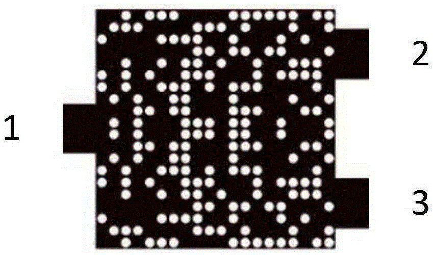
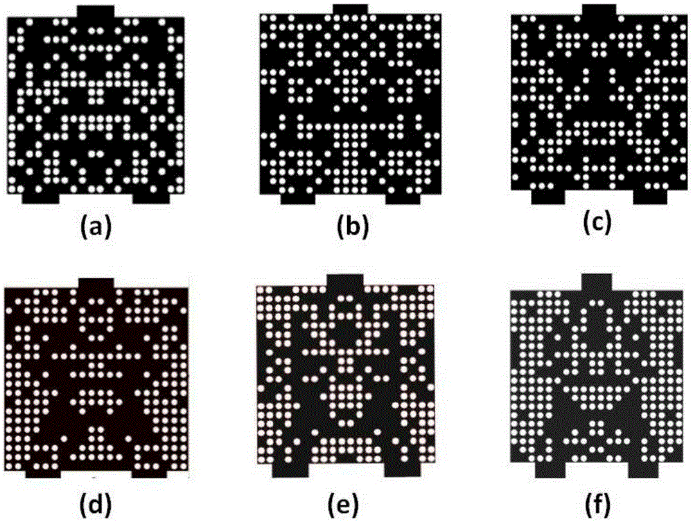
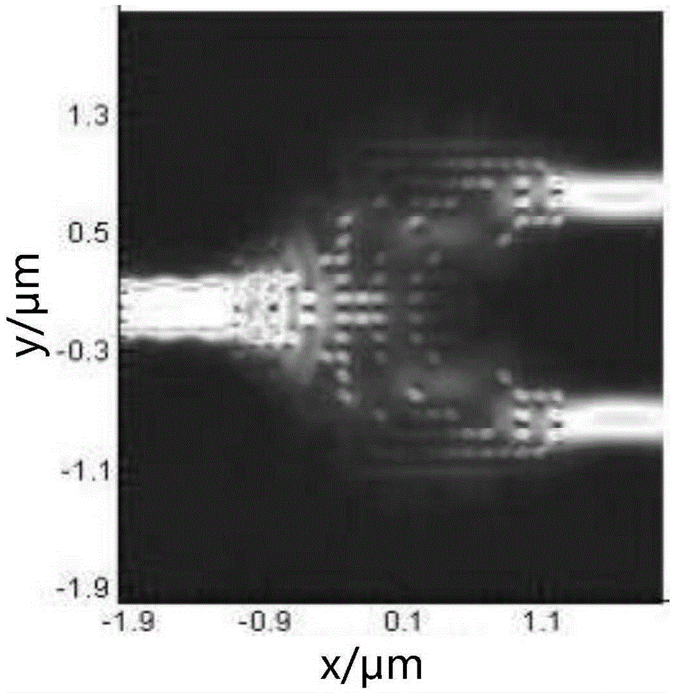
[0027] The structure proposed by the invention includes an input waveguide, two output waveguides, and a square coupling area, and the coupling area includes an air hole array structure with a sub-wavelength size. The incident light enters the coupling area through the input waveguide, and then is divided into two beams of light with the same power and output through two output waveguides respectively.

[0028] In the present invention, the processed material is an ordinary SOI substrate, the input / output waveguide width is 500nm, which is a typical value of the silicon waveguide width, the two out...


PUM


Abstract

The invention discloses a silicon-based metamaterial optical beam splitter and a manufacturing method thereof and belongs to the field of integrated photoenic devices. A 50:50 optical power beam splitter in the prior art is narrow in working broadband, poor in port consistency and high in loss. The optical beam splitter comprises a substrate. The substrate comprises an input waveguide and two output waveguides. A coupling area composed of N*N pixel blocks of the same size are positioned between the input waveguide and the output waveguides. By punching the pixel blocks, a special punching array is formed through an optimization algorithm. Due to the fact that configuration of an air hole array of sub-wavelength sizes can be equivalent to an evenly tempolabile refractive index distribution area, different wavelengths can be guided simultaneously, so that the goal of effectively outputting the different wavelengths at an output port can be achieved, and the goal of large working bandwidth is achieved.

Description

technical field [0001] The invention belongs to the field of integrated photonic devices, and more specifically relates to a silicon-based metamaterial device for realizing optical power splitting and a manufacturing method thereof. Background technique [0002] With the exponential growth of global information exchange, the requirements for high-speed and large-capacity communication systems are getting higher and higher. Optical interconnection technology is the most potential way to overcome communication network transmission bottlenecks. At the same time, the high integration of optical devices is becoming the general trend. Silicon-based optical devices are highly integrated and compatible with the CMOS platform, and are receiving more and more attention. How to reduce device size while still maintaining high performance has always been a major challenge in the field of silicon-based photonics. As an important optical component, the 50:50 optical power beam splitter is...

Claims


Application Information

Patent Timeline
Patent Type & Authority Applications(China)
IPC IPC(8): G02B6/125G02B6/13
CPCG02B6/125G02B6/13
Inventor 张敏明卢鲁璐子周飞亚刘德明
Owner HUAZHONG UNIV OF SCI & TECH
Why Eureka
Try Eureka