Integrated super-quantum LED light-emitting device

A light-emitting device, super quantum technology, applied in the direction of electric solid-state devices, semiconductor devices, electrical components, etc., can solve the problems of chemical corrosion and cleaning process, low production efficiency, not environmental protection, etc., to achieve the optimization of material consumption and production efficiency High, short heat conduction path

Inactive Publication Date: 2016-02-24
SHANGHAI WILLIAMS LIGHTING
View PDF4 Cites 0 Cited by
  • Summary
  • Abstract
  • Description
  • Claims
  • Application Information

AI Technical Summary

Problems solved by technology

[0006] 1) For the final LED light bulb, the LED chip has a long heat conduction path and a large thermal resistance;
[0007] 2) The production process consumes materials and consumes a lot of energy;
[0008] 3) The production process has chemical corrosion and cleaning processes, which is not environmentally friendly;
[0009] 4) LED light sources are complicated in the production and assembly of LED bulbs, and the production efficiency is low

Method used


Image

  • Integrated super-quantum LED light-emitting device
  • Integrated super-quantum LED light-emitting device
  • Integrated super-quantum LED light-emitting device

Examples


Embodiment Construction

[0024] In the following description, many technical details are proposed in order to enable readers to better understand the application. However, those skilled in the art can understand that without these technical details and various changes and modifications based on the following implementation modes, the technical solution claimed in each claim of the present application can be realized.

[0025] In order to make the purpose, technical solution and advantages of the present invention clearer, the following will further describe the implementation of the present invention in detail in conjunction with the accompanying drawings.

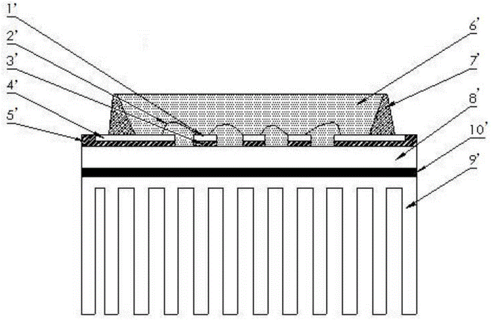
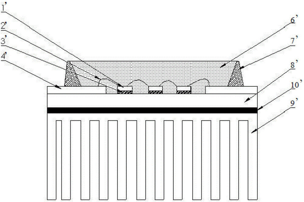
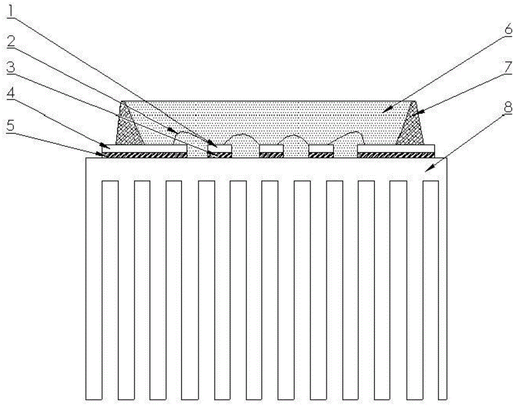
[0026] The first embodiment of the present invention relates to an integrated super quantum LED light emitting device. image 3 It is a structural schematic diagram of the integrated superquantum LED light emitting device. The integrated super quantum LED light emitting device includes a chip 1 , a conductive circuit 4 , an insulating layer 5 and...


PUM


Abstract

The invention relates to an encapsulation technology for an LED light-emitting device, and discloses an integrated super-quantum LED light-emitting device. In the integrated super-quantum LED light-emitting device disclosed by the invention, a radiator substrate is one part of a radiator, and is used as a substrate for supporting a chip and the radiator for heat conduction. The substrate for supporting the chip does not need to be additionally provided, and the substrate is connected with the radiator, so that the chip arranged on the radiator substrate has the shortest heat conduction path and is low in heat resistance; material consumption in the production process is optimized; energy consumption is low; the technology in producing and assembling processes is simple; and the production efficiency is high.

Description

technical field [0001] The invention relates to the packaging technology of LED light-emitting devices, in particular to an integrated super-quantum LED light-emitting device. Background technique [0002] There are two main types of existing COB (chip on board, ChipOnBoard) substrates: [0003] 1) metal substrate (such as figure 1 As shown), the metal with high thermal conductivity, such as pure copper, pure aluminum, etc., is used as the base material of the substrate 8', on which the printed circuit board (4'+5') is bonded. The electrical circuit 4' of the printed circuit board is isolated from the metal substrate by an insulating material 5'. LED (light-emitting diode, Light Emitting Diode) chip 1' is glued on the metal substrate with glue 3', and the metal wire 2' is used to bond the chips for electrical connection. After the connection, the positive and negative electrodes of the chip pass through the printed circuit board (4' +5') is connected to the output termina...

Claims


Application Information

Patent Timeline
IPC IPC(8): H01L25/075H01L33/48H01L33/64
CPCH01L2924/181H01L2224/48137H01L2224/73265H01L2924/00012
Inventor 俞志龙
Owner SHANGHAI WILLIAMS LIGHTING
Why Eureka
Try Eureka