Etching method of double magnetic tunnel junctions

A technology of magnetic tunnel junction and magnetic tunnel, which is applied in the fields of magnetic field controlled resistors, manufacturing/processing of electromagnetic devices, static memory, etc., can solve problems such as short-circuit MTJ stack, failure, and inability to solve DMTJ short-circuit failure, so as to avoid possible The effect of short circuit and large application prospect

Inactive Publication Date: 2016-03-02
CETHIK GRP
View PDF3 Cites 19 Cited by
  • Summary
  • Abstract
  • Description
  • Claims
  • Application Information

AI Technical Summary

Problems solved by technology

[0003] After the top electrode and MTJ stack are prepared on the wafer, they need to be processed and etched into independent units. The by-products of the processing and etching process are easily re-deposited on the side wall of the MTJ, resulting in the connection of the upper and lower electrodes, resulting in a short circuit that causes the MTJ stack to fail.
Although the existing etching process can solve the short circuit problem of single MTJ, it cannot solve the short circuit failure problem of DMTJ.

Method used


Image

  • Etching method of double magnetic tunnel junctions
  • Etching method of double magnetic tunnel junctions
  • Etching method of double magnetic tunnel junctions

Examples


Embodiment 1

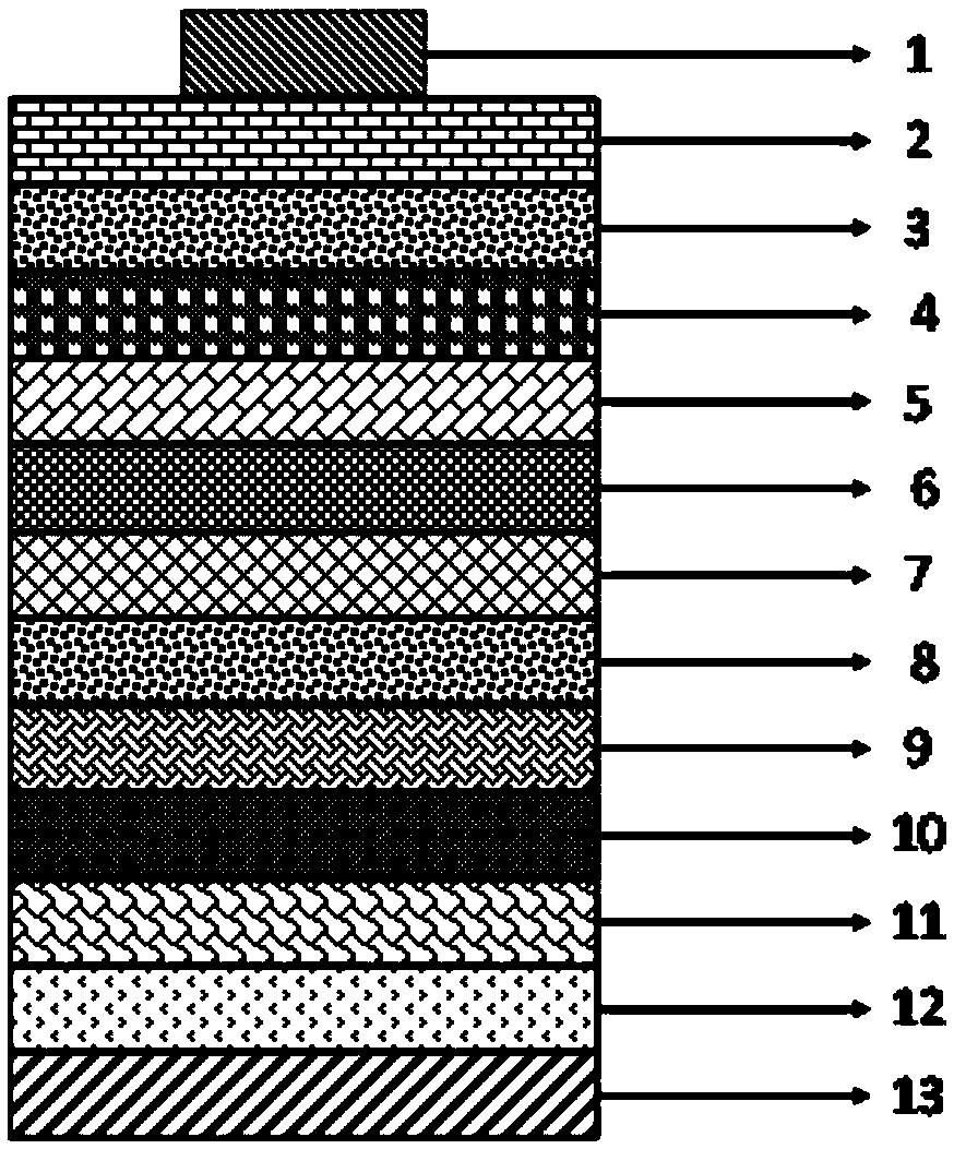
[0028] Embodiment 1: as figure 1 As shown, a photoresist template 1 with a certain shape is prepared in the selected area, the bottom electrode 12, the second antiferromagnetic layer 11, the second pinning layer 10, the second tunneling layer 9, the free layer 8, the first The tunneling layer 7 , the first pinning layer 6 , the first antiferromagnetic layer 5 , the top electrode 4 , the hard template buffer layer 3 and the hard template layer 2 are sequentially deposited on the 13 layers that have been prepared for the front-end process. In this embodiment, in order to simplify the etching process, the hard template buffer layer 3 can be etched under the same etching conditions as the top electrode 4, and the materials for the hard template buffer layer 3 are preferably silicon nitride, silicon carbide and its substitutes. Traditional silicon dioxide, silicon nitride, tantalum nitride and their substitutes are used to prepare the hard template layer 2 . Although figure 1 On...

Embodiment 2

[0032] Embodiment 2: A rectangular photoresist template 1 is prepared in the selected area, the bottom electrode, the second antiferromagnetic layer, the second pinning layer, the second tunneling layer, the free layer, the first tunneling layer, the second A pinning layer, a first antiferromagnetic layer, a top electrode, a hard template buffer layer and a hard template layer are sequentially deposited on the prepared front-end process layer. In this embodiment, in order to simplify the etching process, the hard template buffer layer can be etched under the same etching conditions as the top electrode, and the material of the hard template buffer layer is preferably silicon carbide. Tantalum nitride is used to prepare the hard template layer.

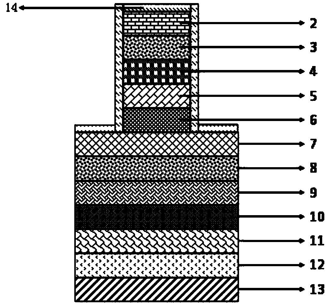
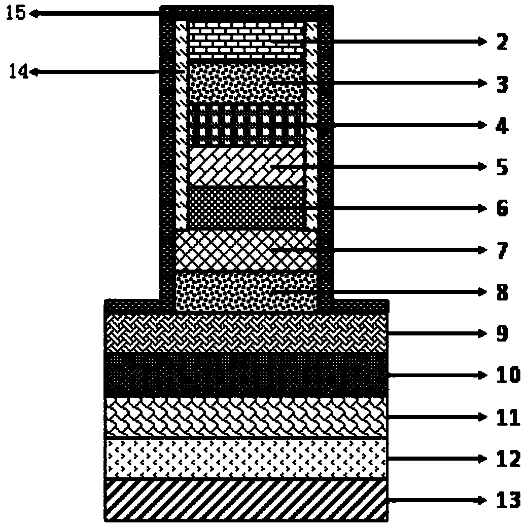
[0033] After the photoresist template layer is removed, the hard template layer replicating the shape of the photoresist template layer is used as a mask to continue etching. When the etching reaches the first tunneling layer, the etc...


PUM


Abstract

The present invention relates to an etching method of double magnetic tunnel junctions. The etching method of double magnetic tunnel junctions comprises the following steps: a hard template and a hard template buffer layer with required shapes are prepared through the photolithography at the portion requiring the maintenance of double magnetic tunnel junction stack; etching begins from a top electrode according to the shape of the hard template, etching the portion requiring etching is performed from the top electrode, the top electrode, a first antiferromagnetic layer and a first pinning layer are etched in turn, etching stops when reaching a first tunneling layer, and a first insulation layer is deposited; etching goes on from a free layer to a second tunneling layer and then stops, and a second insulation layer is deposited; and a second pinning layer and a second antiferromagnetic layer are etched until up to a bottom electrode, and finally residual hard template and hard template buffer layer are etched to obtain a final shape. Through adoption of a second insulation layer and a second insulation layer, the problems the short circuit is easy to happen during processing a double magnetic tunnel junctions and the like; and moreover, the double magnetic tunnel junction stack prepared by the etching method provided by the invention is not reliable to the occurrence of a short circuit phenomenon and is able to process and prepare an MRAM on the basis of the double magnetic tunnel junction stack.

Description

technical field [0001] The invention relates to the technical field of semiconductor storage, in particular to an etching method for a double magnetic tunnel junction. Background technique [0002] Resistive random access memory (RRAM), phase change random access memory (PRAM) and MRAM and other back-end process memories are stored based on the change of the resistance state of the storage unit, which has the advantages of fast speed and non-volatility. The basic storage unit includes the top electrode , resistive medium and bottom electrode three parts. A magnetic tunnel junction (MTJ) resistive dielectric unit for MRAM includes a free layer, a pinned layer and a barrier layer sandwiched therebetween. When the magnetization direction of the free layer is parallel / antiparallel to the magnetization direction of the pinned layer, the resistance state of the MTJ is in the low / high state, corresponding to stored 0 and 1, respectively. In order to reduce the read and write curr...

Claims


Application Information

Patent Timeline
Patent Type & Authority Applications(China)
IPC IPC(8): H01L43/12H01L43/08G11C11/16
CPCG11C11/161
Inventor 左正笏李辉辉徐庶蒋信韩谷昌刘瑞盛孟皓刘波
Owner CETHIK GRP
Why Eureka
Try Eureka