Coating film formation method, base material with transparent conducting film, device and electronic apparatus

A technology of transparent conductive film and coating film, which is applied in the fields of coating film formation, substrates with transparent conductive film, devices and electronic equipment, and can solve the problems of poor material use efficiency, high cost and high price of ITO transparent electrodes, etc.

Active Publication Date: 2016-03-02
KONICA MINOLTA INC
View PDF3 Cites 8 Cited by
  • Summary
  • Abstract
  • Description
  • Claims
  • Application Information

AI Technical Summary

Problems solved by technology

[0008] However, indium used in ITO is a rare metal and is expensive, so it is desirable not to use indium
In addition, there are also problems such as the long production i...

Method used


Image

  • Coating film formation method, base material with transparent conducting film, device and electronic apparatus
  • Coating film formation method, base material with transparent conducting film, device and electronic apparatus
  • Coating film formation method, base material with transparent conducting film, device and electronic apparatus

Examples


Embodiment 1

[0162] (Examples 1 to 6, Comparative Example 1)

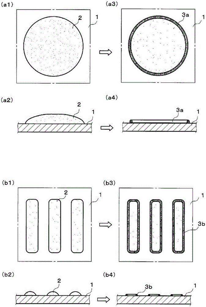
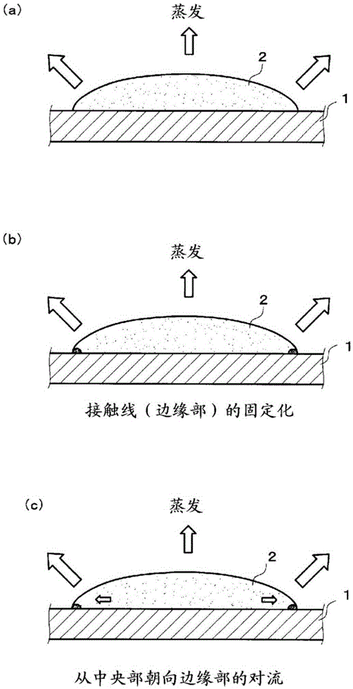
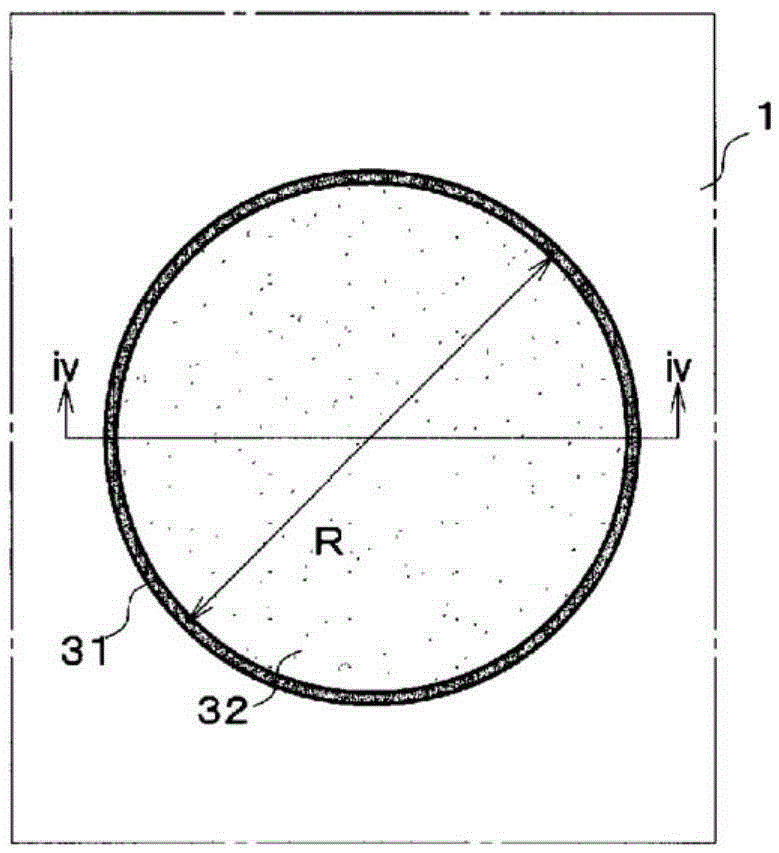
[0163] Using an inkjet head ("KM512L" manufactured by Konica Minolta Corporation; standard droplet volume: 42 pl), the ink of the composition shown in Table 1 was used to attach the droplet to PS-1M manufactured by Shinko Denkisou Co., Ltd. A circular pattern (coating pattern) was formed on the surface of the above-mentioned clear hard coat layer of the PET film (base material) with a clear hard coat layer treated by corona discharge. This pattern was dried, and the solid content was deposited on the edge to form a plurality of fine annular patterns (coating films) with a diameter of 70 μm. These ring-shaped patterns are arranged in a grid at intervals of 282 μm to form an overall pattern ( Figure 7 ). Here, adjacent annular patterns overlap and join each other at edge portions.

[0164] Table 1 shows the results of measuring the total light transmittance and conductivity of the obtained patterns.

Embodiment 7

[0166] By screen printing, using inks of the composition shown in Table 2, line width / space width = 70 μm / 211 μm, and corona discharge-treated PS-1M manufactured by Shinko Electric Keiseo Co., Ltd. with different surface energies A striped pattern (coating pattern) was formed on the transparent hard-coat surface of the transparent hard-coat-attached PET film (substrate). The pattern is dried to form a fine striped pattern (coating film) ( Figure 8 ).

[0167] Table 2 shows the results of measuring the total light transmittance and conductivity of the obtained patterns.

Embodiment 8~13、 comparative example 2

[0169] Using an inkjet head (manufactured by Konica Minolta "KM512L"; the standard droplet volume is 42 pl), using the ink of the composition shown in Table 1, the pitch in the nozzle row direction is 211 μm, and the dot pitch in the scanning direction is 50 μm. The transparent hard-coat surface of the PET film (base material) with a transparent hard-coat layer which corona-discharge-processed using PS-1M by Shinko Denkisou Co., Ltd. was carried out. The respective droplets on the substrate were united to form a striped pattern (coating pattern) similar to that of Example 7. By drying the pattern, the solid content is deposited on the edge to form a fine striped pattern (coating film) ( Figure 8 ).

[0170] Table 2 shows the results of measuring the total light transmittance and conductivity of the obtained patterns.

[0171]

[0172] ・Substrate heating method: After the coating film is formed, the substrate is heated with a heating plate.

[0173] · Substrate surface te...


PUM


Abstract

The purpose of the present invention is to provide a coating film formation method that is capable of stably forming a pattern that includes fine wires having a fine wire width, and is capable of reducing solid residue outside a prescribed patterning position for a fine wire part. In the coating film formation method of the present invention, a coating film with a functional material selectively deposited on an edge part is formed by coating the top of a base material (1) with a liquid that includes the functional material to form a pattern (2) and then drying the pattern. The functional material is caused to deposit on the edge part of the coating film because the liquid includes a solvent with a high degree of affinity for the functional material and a solvent with a low degree of affinity for the functional material.

Description

technical field [0001] The present invention relates to a coating film forming method for forming a coating film in which a functional material is deposited on an edge, a substrate with a transparent conductive film using the coating film formed by the coating film forming method, a device, and an electronic device. Background technique [0002] In recent years, higher functionality and higher densities of devices have been developed, and techniques for forming microscopic patterns containing functional materials have been sought. At the same time, cost reduction and simplification of manufacturing processes are also required. [0003] As the above-mentioned pattern forming method, it has been proposed to form a pattern by a printing method. However, using various printing methods, the limit is only to form a pattern with a line width of about 20 μm, and it is difficult to meet the required miniaturization. [0004] Patent Document 1 discloses that by utilizing convection i...

Claims


Application Information

Patent Timeline
IPC IPC(8): B05D1/26B05D5/12B05D7/00H01B5/14H05K3/10
CPCH01L31/1884H05K1/092H05K3/125H05K3/227H05K2201/0108H05K2201/09736H05K2201/098H05K2203/0545H05K2203/0783H05K2203/1105H05K2203/1173H05K2203/1581
Inventor 新妻直人大屋秀信牛久正幸山内正好
Owner KONICA MINOLTA INC
Why Eureka
Try Eureka