Self-assembly orderly patterning growing preparing method of rubrene films
A self-assembly, rubrene technology, applied in ion implantation plating, metal material coating process, coating and other directions, can solve the problems of reducing film mobility, destroying film structure, and high process cost
- Summary
- Abstract
- Description
- Claims
- Application Information
AI Technical Summary
Problems solved by technology
Method used
Image
Examples
Embodiment Construction
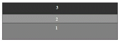
[0008] Such as image 3 As shown, Si substrate (1), the substrate temperature is 20℃; SiO 2 The insulating layer (2) has a thickness of 300nm; the rubrene layer (3) has a thickness of 50nm.
[0009] The specific realization process: the substrate is composed of substrate Si (1) and a layer of 300nm thick SiO on its surface 2 (2) Composition; clean the substrate and put it into the reaction chamber of the seven-station OEL / EL photoelectric thin film joint preparation system; the vacuum degree of the reaction chamber is evacuated to less than 6.0×10 -4 Pa; a layer of rubrene was vacuum evaporated on the substrate with a thickness of 50nm, and the substrate temperature was 20°C. First, it is deposited according to the evaporation rate of 2nm / min, with a thickness of about 10nm, on SiO 2 The dot-like aggregation of rubrene molecules is formed on the layer; then stop for 5 minutes to realize the self-assembly arrangement of molecules; then continue to deposit at the evaporation ...
PUM
| Property | Measurement | Unit |
|---|---|---|
| thickness | aaaaa | aaaaa |
Abstract
Description
Claims
Application Information


