Manufacturing method of low-temperature ohmic contact of III group nitride electronic device

A technology for ohmic contact and electronic devices, which is applied in semiconductor/solid-state device manufacturing, electrical components, semiconductor devices, etc. It can solve problems such as surface degradation of Group III nitrides, affect device dynamic characteristics and power output capabilities, and increase ohmic contact. area, reduce the contact barrier, and increase the effect of electron tunneling probability

Inactive Publication Date: 2016-03-09
INST OF MICROELECTRONICS CHINESE ACAD OF SCI
View PDF2 Cites 6 Cited by
  • Summary
  • Abstract
  • Description
  • Claims
  • Application Information

AI Technical Summary

Problems solved by technology

[0004] In view of this, the main purpose of the present invention is to provide a method for making low-temperature ohmic contacts of III-nitride electronic devices, so as to reduce the ohmic contact resistance,

Method used


Image

  • Manufacturing method of low-temperature ohmic contact of III group nitride electronic device
  • Manufacturing method of low-temperature ohmic contact of III group nitride electronic device
  • Manufacturing method of low-temperature ohmic contact of III group nitride electronic device

Examples


Embodiment 1

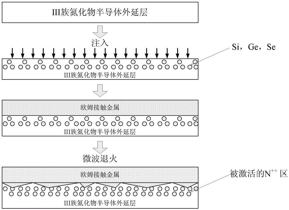
[0024] Such as figure 1 and figure 2 as shown, figure 1 It is a flow chart of the manufacturing process of the low-temperature ohmic contact of the III-nitride electronic device according to the first embodiment of the present invention, figure 2 It is a flow chart of a method for manufacturing a low-temperature ohmic contact of a III-nitride electronic device according to a first embodiment of the present invention, and the method includes the following steps:

[0025] Step 1: Implanting N-type impurities in the III-nitride ohmic contact region; in this step, the N-type impurities can be Si elements, Ge elements, Se elements or co-doped implants of the above elements and N elements.

[0026] Step 2: Deposit ohmic metal on the III-nitride ohmic contact area implanted with N-type impurities; in this step, the ohmic metal can be gold-containing multilayer metal or gold-free multilayer metal, wherein gold The multilayer metal is any structure in Ti / Al / Ni / Au structure, Ti / Al / ...

Embodiment 2

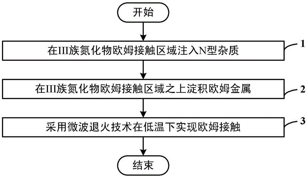
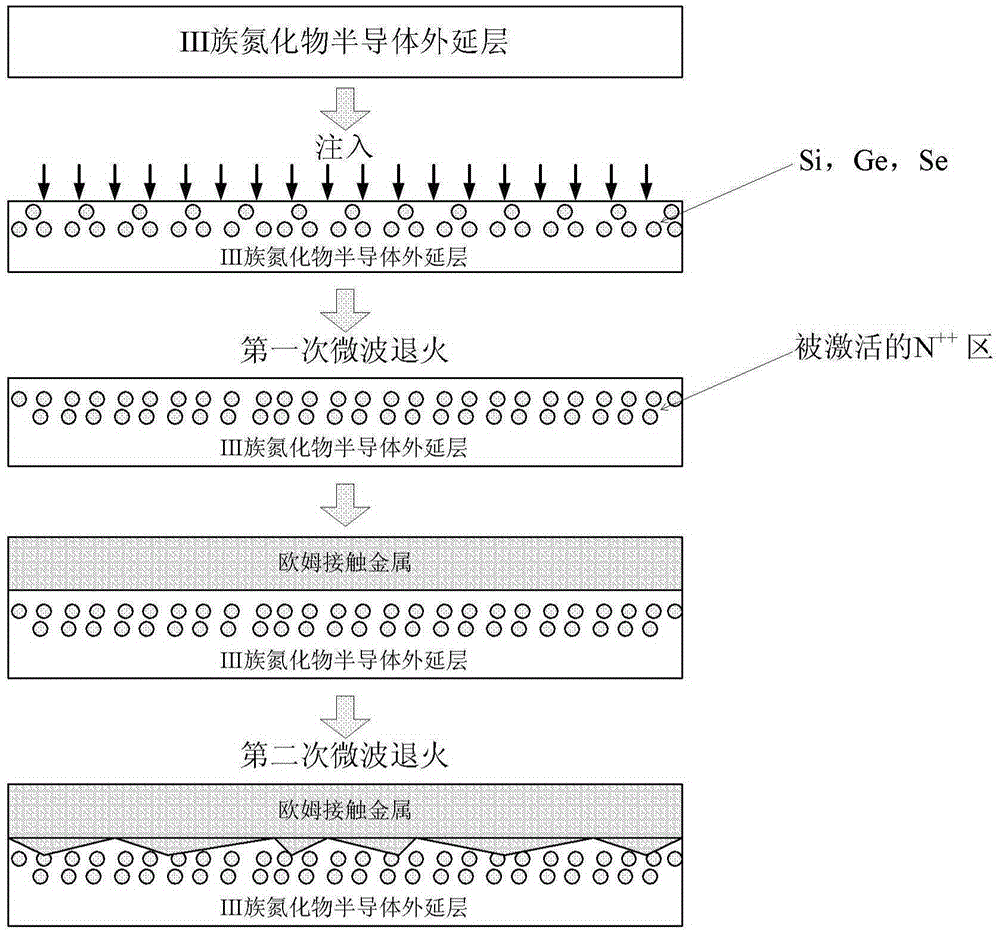
[0029] Such as image 3 and Figure 4 as shown, image 3 It is a flow chart of the manufacturing process of the low-temperature ohmic contact of the III-nitride electronic device according to the second embodiment of the present invention, Figure 4 It is a flowchart of a method for manufacturing a low-temperature ohmic contact of a III-nitride electronic device according to a second embodiment of the present invention, and the method includes the following steps:

[0030] Step a: Implanting N-type impurities in the III-nitride ohmic contact region; in this step, the N-type impurities may be Si elements, Ge elements, Se elements or co-doped implants of the above elements and N elements.

[0031] Step b: Use microwave annealing technology to activate the implanted N-type impurities; in this step, use microwave annealing technology to activate the N-type impurities at a low temperature below 800°C to form N ++ doping.

[0032]Step c: Deposit ohmic metal on the III-nitride oh...


PUM


Abstract

The invention discloses a manufacturing method of low-temperature ohmic contact of a III group nitride electronic device. The manufacturing method comprises the steps of: injecting N type impurities in a III group nitride ohmic contact region; depositing ohmic metal on the III group nitride ohmic contact region injected with the N type impurities; and adopting a microwave annealing technology to achieve ohmic contact at low temperature. After the N type impurities are injected to the III group nitride ohmic contact region, the manufacturing method further comprises the step of adopting the microwave annealing technology to activate the injected N type impurities. The microwave annealing technology utilizes the microwave annealing technology to achieve the low-temperature activation of the injected N type impurities in III group nitrides, so as to form an N type heavily-doped layer, increase electronic tunnelling probability, and reduce ohmic contact resistance; furthermore, the manufacturing method can enhance the interface reaction between the ohmic metal and the III group nitride semiconductor, reduce contact-potential barrier, improve ohmic contact area, and further reduce the contact resistance.

Description

technical field [0001] The invention relates to the technical field of manufacturing low-temperature ohmic contacts of semiconductor devices, in particular to a method for manufacturing low-temperature ohmic contacts of III-nitride electronic devices whose temperature is lower than 800°C. Background technique [0002] Group III nitride wide bandgap semiconductors are currently one of the hot candidates for RF microwave power amplifier and power electronics applications. At present, the ohmic contact of III-nitride electronic devices is mainly realized by rapid thermal annealing method at high temperature. The annealing temperature is generally higher than 800°C, which belongs to high-temperature annealing technology. High-temperature annealing above 800°C will generally cause surface degradation of group III nitrides, resulting in more surface states, which directly affect the dynamic characteristics and power output capability of the device. Therefore, the development of a...

Claims


Application Information

Patent Timeline
IPC IPC(8): H01L21/28H01L29/45H01L21/324
CPCH01L21/28H01L21/3245H01L29/454
Inventor 黄森刘新宇王鑫华魏珂包琦龙罗军赵超
Owner INST OF MICROELECTRONICS CHINESE ACAD OF SCI
Why Eureka
Try Eureka