Silicon-based gallium nitride high-power radio frequency device based on gold-free process and preparation method thereof

A radio frequency device, silicon-based nitrogen technology, applied in the field of microelectronics, can solve the problems of inability to integrate heterogeneous Si-based CMOS control components, incompatibility with Si-based CMOS processes, and high cost of a single SiC-based GaN, so as to improve power-added efficiency , Reduce the impact of device performance, improve efficiency and power density

Pending Publication Date: 2022-07-01
XIDIAN UNIV
View PDF0 Cites 0 Cited by
  • Summary
  • Abstract
  • Description
  • Claims
  • Application Information

AI Technical Summary

Problems solved by technology

[0003] At present, at home and abroad, the gold-containing process is widely used in the device process to make SiC-based GaN devices, which can achieve higher power. These methods have the following problems: (1) The cost of a single SiC-based GaN is high, and the wafer Small size leads to low productivity and low tape-out efficiency; (2) SiC-based GaN adopts traditional gold-containing process and cannot be compatible with Si-based CMOS process, and cannot be heterogeneously integrated with Si-based CMOS control components

Method used


Image

  • Silicon-based gallium nitride high-power radio frequency device based on gold-free process and preparation method thereof
  • Silicon-based gallium nitride high-power radio frequency device based on gold-free process and preparation method thereof
  • Silicon-based gallium nitride high-power radio frequency device based on gold-free process and preparation method thereof

Examples


Embodiment 1

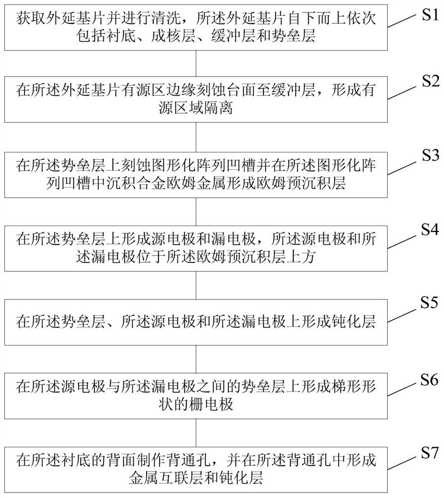
[0053] See figure 1 , Figure 2a to Figure 2k , figure 1 This is a flow chart of a method for preparing a high-power GaN-on-silicon high-power radio frequency device based on a gold-free process provided by an embodiment of the present invention, Figure 2a to Figure 2k A schematic diagram of a preparation process of a silicon-based gallium nitride high-power radio frequency device based on a gold-free process provided by an embodiment of the present invention. The preparation method of this embodiment includes:

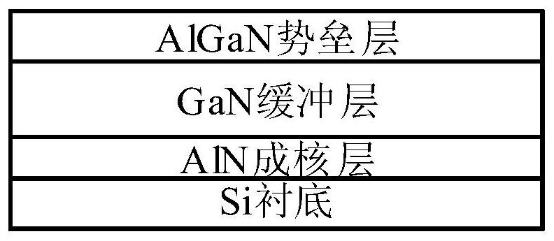
[0054] S1: Obtaining and cleaning an epitaxial substrate, the epitaxial substrate including a substrate, a nucleation layer, a buffer layer and a barrier layer in sequence from bottom to top.

[0055] Specifically, the device of this embodiment is fabricated on an epitaxial substrate that already contains a substrate, a nucleation layer, a buffer layer, and a barrier layer, wherein the substrate, the nucleation layer, the buffer layer, and the barrier layer are fo...

Embodiment 2

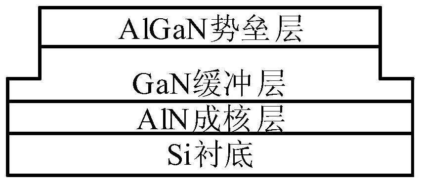
[0133] On the basis of the above embodiment, this embodiment provides a high-power radio frequency device of gallium nitride on silicon based on a gold-free process. See image 3 , image 3 It is a schematic structural diagram of a silicon-based gallium nitride high-power radio frequency device based on a gold-free process provided by an embodiment of the present invention. The silicon-based GaN high-power radio frequency device of this embodiment includes that the power device includes a Si substrate layer 1, an AlN nucleation layer 2, a GaN buffer layer 3, and an AlGaN barrier layer 4 that are sequentially arranged from bottom to top, wherein, Two columns of patterned array grooves 5 arranged in parallel are formed on the upper surface of the AlGaN barrier layer 4 , source electrodes 6 and drain electrodes 7 are respectively provided on both sides of the upper surface of the AlGaN barrier layer 4 , and the two columns of patterned array grooves 5 are respectively located b...


PUM

PropertyMeasurementUnit
Angleaaaaaaaaaa
Thicknessaaaaaaaaaa
Thicknessaaaaaaaaaa

Abstract

The invention discloses a silicon-based gallium nitride high-power radio frequency device based on a gold-free process and a preparation method thereof, and the preparation method comprises the steps: obtaining and cleaning an epitaxial substrate which sequentially comprises a substrate, a nucleating layer, a buffer layer and a barrier layer from bottom to top; etching a table surface from the edge of the active region of the epitaxial substrate to the buffer layer to form active region isolation; etching a patterned array groove in the barrier layer, and depositing alloy ohmic metal in the patterned array groove to form an ohmic pre-deposition layer; forming a source electrode and a drain electrode on the barrier layer, wherein the source electrode and the drain electrode are located above the ohmic pre-deposition layer; forming a passivation layer on the barrier layer, the source electrode and the drain electrode; forming a trapezoidal gate electrode on the barrier layer between the source electrode and the drain electrode; and manufacturing a back through hole, and forming a source electrode interconnection layer and a passivation layer in the back through hole. The power device adopts the ohmic pre-deposition layer and the grid electrode with the inclined field plate, so that the contact resistance is reduced, and the channel electric field distribution is improved.

Description

technical field [0001] The invention belongs to the technical field of microelectronics, and in particular relates to a silicon-based gallium nitride high-power radio frequency device based on a gold-free process and a preparation method thereof. The silicon-based gallium nitride high-power radio frequency device can be used for 5G base station systems, satellite navigation, in the radar system. Background technique [0002] Due to the large band gap, high breakdown field strength, and the ability to obtain a high-concentration two-dimensional electron gas channel by forming a heterojunction with AlGaN, GaN has a high breakdown voltage and low on-resistance that exceed the limits of Si and SiC. Therefore, AlGaN / GaN HEMTs (High Electron Mobility Transistor, high electron mobility transistors) have great advantages in power switching applications. Due to the poor thermal conductivity of sapphire and the high cost of SiC, the power application of high-power AlGaN / GaN HEMTs bas...

Claims


Application Information

Patent Timeline
IPC IPC(8): H01L29/20H01L29/417H01L29/45H01L29/423H01L29/40H01L29/778H01L21/335
CPCH01L29/2003H01L29/41725H01L29/452H01L29/42312H01L29/402H01L29/778H01L29/66462
Inventor 马晓华芦浩侯斌杨凌司泽艳杜佳乐郝跃
Owner XIDIAN UNIV
Why Eureka
Try Eureka