
Absorption region structure for unitraveling carrier photodiode

A photodiode, single-row carrier technology, used in circuits, electrical components, semiconductor devices, etc., can solve the problems of holes not leaving in time, limiting device bandwidth, and low drift speed, shortening transit time and accelerating drift. , the effect of enhancing the electric field strength

Inactive Publication Date: 2016-03-09
SHANGHAI INST OF MICROSYSTEM & INFORMATION TECH CHINESE ACAD OF SCI
View PDF3 Cites 12 Cited by
  • Summary
  • Abstract
  • Description
  • Claims
  • Application Information

AI Technical Summary

Problems solved by technology

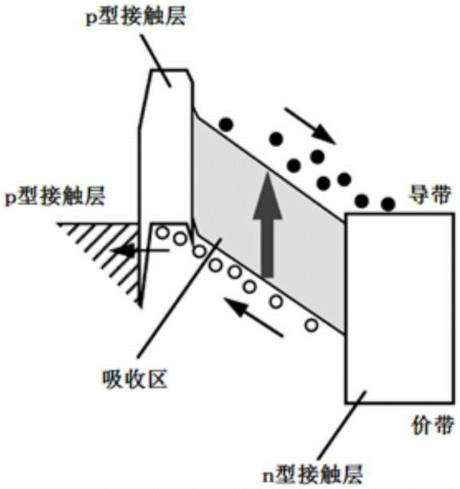
However, the drift speed of holes is much lower than that of electrons, which limits the bandwidth of the device; at the same time, when the incident light power becomes larger, a large number of holes generated cannot leave the depletion region in time, and the accumulation of holes causes space charge effect, causing the device to enter saturation
Due to the above limitations, the response bandwidth of a general high-speed PIN-PD is tens of GHz, which is slightly insufficient if it is to be applied in the terahertz (100GHz-10THz) field

Method used


Image

  • Absorption region structure for unitraveling carrier photodiode
  • Absorption region structure for unitraveling carrier photodiode
  • Absorption region structure for unitraveling carrier photodiode

Examples


Embodiment Construction

[0032] Embodiments of the present invention are described below through specific examples, and those skilled in the art can easily understand other advantages and effects of the present invention from the content disclosed in this specification. The present invention can also be implemented or applied through other different specific implementation modes, and various modifications or changes can be made to the details in this specification based on different viewpoints and applications without departing from the spirit of the present invention.

[0033] see Figure 3a ~ Figure 5 . It should be noted that the diagrams provided in this embodiment are only schematically illustrating the basic idea of ​​the present invention, so that only the components related to the present invention are shown in the diagrams rather than the number, shape and Dimensional drawing, the type, quantity and proportion of each component can be changed arbitrarily during actual implementation, and the...


PUM


Abstract

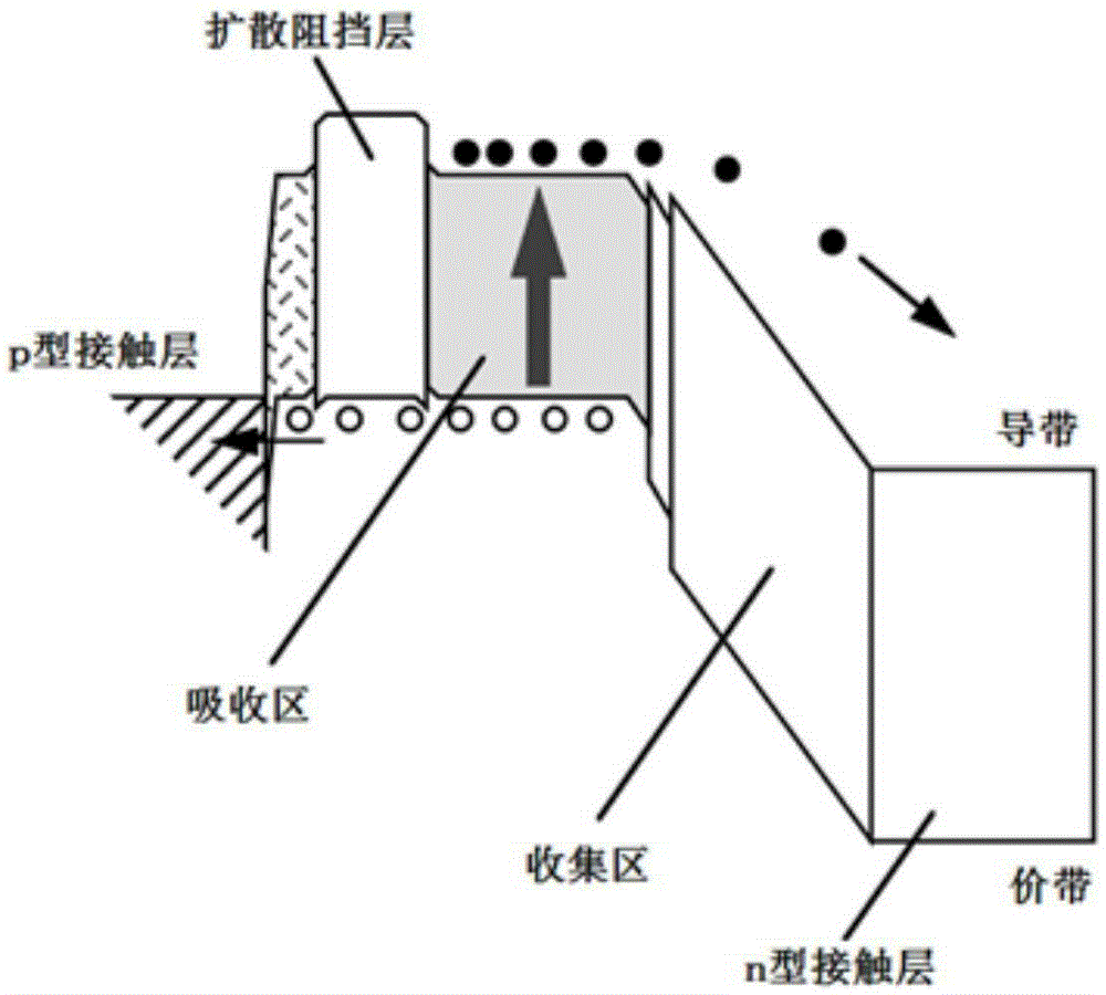
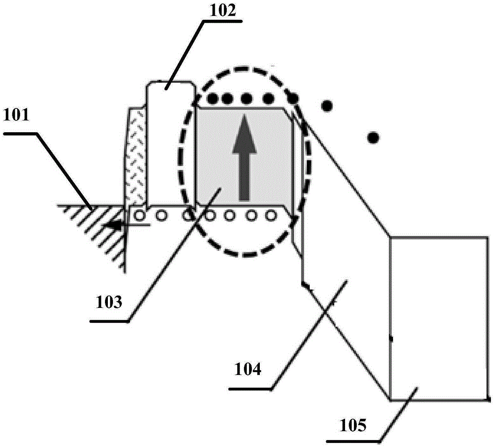
The invention provides an absorption region structure for a unitraveling carrier photodiode. The absorption region structure employs an In1-xGaxAsyP1-y material for growth, wherein the x and y express material components of a Ga element and a As element, the x is larger than 0 and is less than 1 and the y is larger than 0 and is less than or equal to 1; and the component parameters x and y change in a linear gradient mode or in a step type gradient mode, so that the gradient change of the forbidden band width in the absorption region is realized. Moreover, with selection of the component parameters x and y, the lattice constant of the In1-xGaxAsyP1-y material matches InP and the forbidden band width is not larger than that of photon energy of laser with the wavelength of 1.5 microns. According to the invention, with utilization of a built-in electric field introduced by a gradient energy band structure, the electric field intensity in the absorption region can be enhanced obviously; and the drift of electrons can be accelerated effectively based on the enhanced electric field and the transition time at the absorption region can be shortened. Therefore, the electron transition time in the absorption region of the unitraveling carrier photodiode can be reduced effectively. And utilization of the absorption region structure has the great significance in improving the bandwidth of the device and realizing the ultra-high-speed wireless communication system based on the device.

Description

technical field [0001] The invention relates to a design method of a single-row carrier photodiode, in particular to an absorption region structure for a single-row carrier photodiode. Background technique [0002] Photodiode (Photodiode, PD) is an important photoelectric conversion device, which has a wide range of applications in the national economy and military applications. It is the core device of application systems such as optical fiber communication, ultra-wideband wireless communication, missile guidance, infrared imaging and remote sensing. . PD has two important indicators: saturation current and response bandwidth. The former determines the output power, and the latter reflects the high-frequency response capability of the device. Many researches on PD are carried out around improving these two performance indicators. PDs with large saturation current and fast response can meet more application requirements, which is especially important for high-speed communi...

Claims


Application Information

Patent Timeline
Patent Type & Authority Applications(China)
IPC IPC(8): H01L31/0304H01L31/0352H01L31/10
CPCH01L31/03046H01L31/035272H01L31/10
Inventor 张戎曹俊诚邵棣祥
Owner SHANGHAI INST OF MICROSYSTEM & INFORMATION TECH CHINESE ACAD OF SCI
Learn More