Method for removing pad defect

A pad and defect technology, applied in the field of pad defect removal, can solve the problems of limited defect removal capability, high cost, pad metal damage, etc., to reduce pits defects, reduce pad damage, and save rework costs Effect

Inactive Publication Date: 2016-03-23
WUHAN XINXIN SEMICON MFG CO LTD
View PDF5 Cites 7 Cited by
  • Summary
  • Abstract
  • Description
  • Claims
  • Application Information

AI Technical Summary

Problems solved by technology

[0004] At present, there are two conventional ways to rework and remove (rework) pad defects: the first is to first cover the photoresist in the non-PAD area; secondly, to bombard the surface with high-energy ions; Passivation treatment, this method can effectively remove pad defects, but the disadvantages of this method are that the removal process is complicated, the cost is high, and it may also cause dry etching (dryetch) machine parts (parts) damage (damage) )
The second is to use DSP solution containing hydrofluoric acid (HFDSP) (HF+H2SO4+H2O2) to dissolve and flush defects in the spin process. The disadvantage of this method is that the ability to remove defects is limited. If the time is prolonged, it will cause Pad metal Too much damage, even damage to the pad itself, these are not expected by those skilled in the art

Method used


Image

  • Method for removing pad defect

Examples


Embodiment Construction

[0023] The present invention will be further described below in conjunction with the accompanying drawings and specific embodiments, but not as a limitation of the present invention.

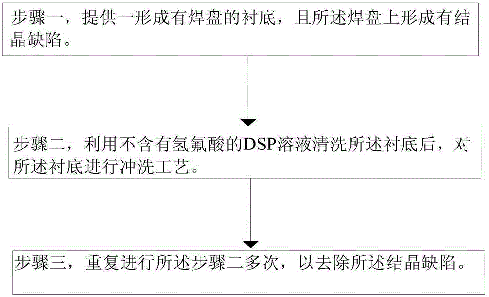
[0024] Such as figure 1 As shown, this embodiment relates to a method for removing pad defects, including:

[0025] Step 1, providing a substrate with pads formed, and crystal defects formed on the pads; since the technology of the substrate with pads can be well known to those skilled in the art, its specific preparation process is in I won't go into details here.

[0026] In a preferred embodiment of the present invention, the pad is an aluminum pad, and correspondingly, the crystal defect is a compound containing fluorine (F), oxygen (O) and aluminum (Al). The mechanism of the crystal defect formation is: the aluminum pad and its oxide react to form aluminum hydroxide in the presence of fluoride ions and water vapor, and then react with H+F- to form the compound containing fluorine, oxygen ...


PUM


Abstract

The present invention relates to the technical field of semiconductor manufacturing and particularly relates to a method for removing a pad defect. After a DSP solution without hydrofluoric acid is used to clean a pad, the pad is subjected to washing process, the cleaning and washing processes are repeated for many times to remove the pad defect, since the DSP solution does not contain the hydrofluoric acid, the pad damage in the process of removing the pad defect can be reduced, and pit defects are reduced. Since the DSP high and low speed matching is used, the streaming can be increased to increase chemical cleaning ability, the mode of repeated cleaning and washing is employed, the effect of the sulfuric acid and hydrogen peroxide in the solution can be improved, thus the pad defect can be effectively removed, scrap can be reduced, the yield is improved, and the cost os rework is saved.

Description

technical field [0001] The invention relates to the technical field of semiconductor manufacturing, in particular to a method for removing pad defects. Background technique [0002] In the semiconductor manufacturing process, pad crystal defect (Pad Crystal defect) is a common process defect. This defect will be judged as abnormal appearance during the IC chip shipment visual inspection process. If it cannot be reworked and removed, there will be a risk of scrapping. [0003] The pad defect is manifested as a protrusion of the pad in the case of OM (visual inspection), and it is manifested as a product of abnormal growth of Al under SEM (under the electron microscope). [0004] At present, there are two conventional ways to rework and remove (rework) pad defects: the first is to first cover the photoresist in the non-PAD area; secondly, to bombard the surface with high-energy ions; Passivation treatment, this method can effectively remove pad defects, but the disadvantages ...

Claims


Application Information

Patent Timeline
Patent Type & Authority Applications(China)
IPC IPC(8): H01L21/02
CPCY02P80/30H01L21/02068
Inventor 胡海波汪亚军
Owner WUHAN XINXIN SEMICON MFG CO LTD
Why Eureka
Try Eureka