Method for manufacturing transistor based on metal nano-dot trench, and prepared product

A metal nano-transistor technology, applied in the fields of semiconductor/solid-state device manufacturing, nanotechnology, semiconductor devices, etc., can solve problems such as the method of manufacturing fin field effect transistors that has not yet been proposed, and achieve the effect of low power consumption and small area

Active Publication Date: 2016-03-30
SEMICON MFG INT (SHANGHAI) CORP
View PDF4 Cites 4 Cited by
  • Summary
  • Abstract
  • Description
  • Claims
  • Application Information

AI Technical Summary

Problems solved by technology

[0007] However, the industry has not yet proposed a method for fabrica

Method used


Image

  • Method for manufacturing transistor based on metal nano-dot trench, and prepared product
  • Method for manufacturing transistor based on metal nano-dot trench, and prepared product
  • Method for manufacturing transistor based on metal nano-dot trench, and prepared product

Examples


Embodiment Construction

[0029] In the following description, the present invention is described with reference to various examples. One skilled in the art will recognize, however, that the various embodiments may be practiced without one or more of the specific details, or with other alternative and / or additional methods, materials, or components. In other instances, well-known structures, materials, or operations are not shown or described in detail so as not to obscure aspects of the various embodiments of the invention. Similarly, for purposes of explanation, specific quantities, materials and configurations are set forth in order to provide a thorough understanding of embodiments of the invention. However, the invention may be practiced without these specific details. Furthermore, it should be understood that the various embodiments shown in the drawings are illustrative representations and are not necessarily drawn to scale.

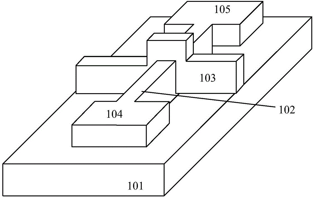
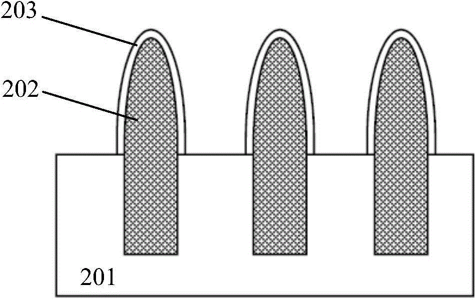
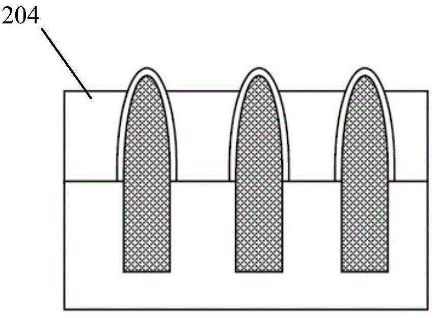
[0030] The present inventors conceived a method for fabricating a f...


PUM


Abstract

The invention discloses a method for manufacturing a transistor based on a metal nano-dot trench, and a prepared product. The method can manufacture a trench with a metal nano dot, thereby obtaining a transistor which is prepared without a semiconductor. The method comprises the steps: forming fin-shaped structures on a substrate; forming insulating layers on the surfaces of the fin-shaped structures; filling a gap between the fin-shaped structures with gap filling materials; exposing the tops of the fin-shaped structures; forming a metal nano dot array at the tops of the gap filling materials and the fin-shaped structures; and removing the gap filling materials and the metal nano dots on the gap filling materials, so as to form a structure which is only provided with the metal nano dots at the tops of the fin-shaped structures.

Description

technical field [0001] The invention relates to the manufacturing field of semiconductor devices, in particular to a method for forming a fin field effect transistor based on a metal nano-dot channel, and a product manufactured by the method. Background technique [0002] With the rapid development of semiconductor manufacturing technology, the feature size of transistors has entered the nanoscale. Since it took three to four years for the semiconductor industry to switch from a 0.18-micron process to a 0.13-micron process, it has been proved that improving the performance of current mainstream semiconductor devices through proportional scaling is subject to more and more physical and technological limitations. In order to enable integrated circuit technology to continue the development speed revealed by Moore's Law, transistors with new materials, new structures and new properties must be developed. [0003] Currently, a multi-gate field-effect transistor (MuGFET) has been...

Claims


Application Information

Patent Timeline
IPC IPC(8): H01L21/336H01L29/10B82Y40/00
Inventor 张海洋
Owner SEMICON MFG INT (SHANGHAI) CORP
Why Eureka
Try Eureka