
Manufacturing method for pre-packaged lead frame

A manufacturing method and a technology of encapsulating leads, which are applied in semiconductor/solid-state device manufacturing, electrical components, electrical solid-state devices, etc., can solve the problems of lead frame testing, low testing efficiency, difficulty in mass production, etc., and achieve short alignment time , Improve test efficiency and reduce damage

Inactive Publication Date: 2016-04-06
NINGBO KANGQIANG ELECTRONICS CO LTD
View PDF7 Cites 7 Cited by
  • Summary
  • Abstract
  • Description
  • Claims
  • Application Information

AI Technical Summary

Problems solved by technology

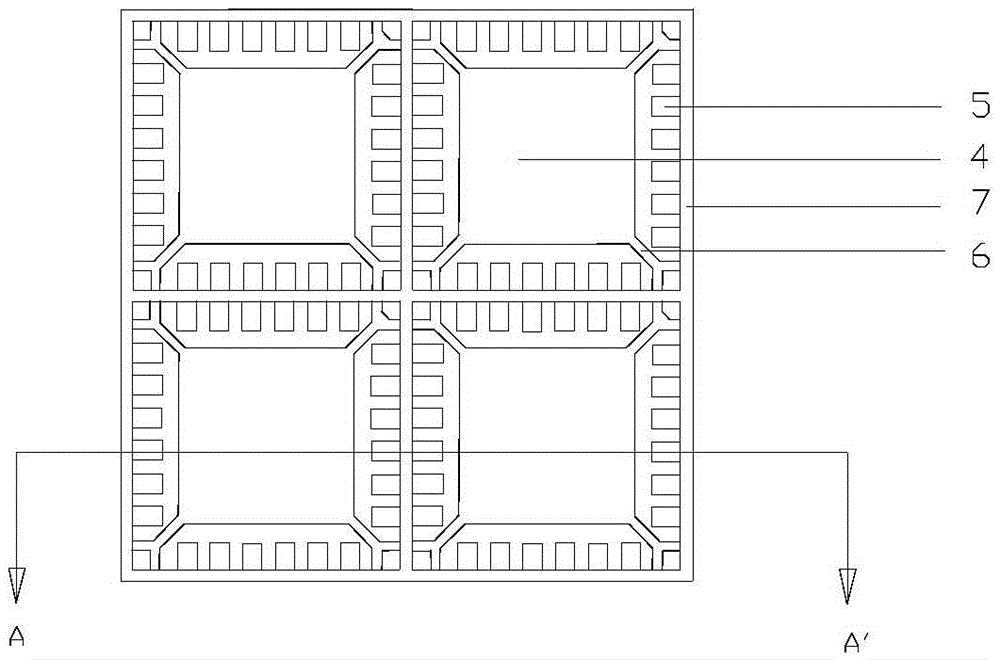
But this method still retains the follow-up metal cutting process, so that the test of the whole piece of lead frame cannot be carried out during the test, because the existence of the middle rib 7 makes the pins 5 of the carrying unit be short-circuited, and the pins of each carrying unit must be connected to each other. After the middle ribs 7 are cut off, they can be tested one by one. The test efficiency is very low. In addition, because the half-etched area of ​​the middle ribs 7 will be filled with plastic seals in the subsequent injection molding process, it is easy to cause cutting and molding. Delamination of the metal layer and the plastic layer occurs under the action
[0004] At present, there is another method for manufacturing the lead frame, which does not need to set the middle rib 7, but realizes the area to be etched by performing a half-etch on the front side and the back side respectively. Although this method does not need to cut metal in the subsequent process, However, after the half-etching of the front side, when the half-etching of the back side is performed again, since there are many areas to be etched, a long alignment time is required, which will cause a decrease in production efficiency on the one hand and make it difficult to achieve mass production. Longer alignment times also exacerbate unwanted side erosion during etching

Method used


Image

  • Manufacturing method for pre-packaged lead frame
  • Manufacturing method for pre-packaged lead frame
  • Manufacturing method for pre-packaged lead frame

Examples


Embodiment

[0022] This embodiment provides a method for manufacturing an integrated circuit element that includes a method for manufacturing a pre-encapsulated lead frame of the present invention, which undergoes the following steps in sequence:

[0023] (1) The first etching: provide a metal substrate such as Figure 2a As shown, the metal substrate 1 can be made of a metal with good conductivity, such as copper, iron, aluminum, nickel, zinc or its alloys, etc., and two etching methods are performed on the front side of the metal substrate 1: full etching and partial etching, to obtain Figure 2b , full etching is used to form several etched holes 3 to form the chip seat 4, pin 5, seat post 6 and middle rib 7 of each carrying unit, and the chip seat 4, pin 5, seat post 6 and middle rib The shape structure of 7 adopts the shape structure of the existing QFN lead frame, such as figure 1 As shown, the partial etching is the first partial etching carried out along the front face 2 of the m...


PUM


Abstract

A manufacturing method for a pre-packaged lead frame is disclosed. The manufacturing method is characterized by comprising the following steps: (1) etching for the first time, wherein the front surface of a metal substrate is subjected to two etching ways, including whole etching and partial etching; the whole etching is for forming multiple etched etching holes for forming chip bases, pins, base columns and middle ribs of each bearing unit; and the partial etching is carried out by performing a first time etching along the front surface of the middle rib to remove a part of the thickness of the middle rib; (2) pre-packaging, wherein the etching holes, and the removed part of the middle rib in the first time are injected with first plastic package part for performing pre-packaging; and (3) etching for the second time, wherein partial etching for the second time is performed along the back surface of the middle rib to remove the residual of the middle rib. According to the manufacturing method for the pre-packaged lead frame, metal cutting is not required; the cutting process does not cause layering; and small secondary cutting region, short alignment time, low manufacturing cost and high production efficiency are realized.

Description

technical field [0001] The invention relates to the technical field of lead frames, in particular to a method for manufacturing a pre-encapsulated lead frame. Background technique [0002] In the field of semiconductor manufacturing technology, the lead frame, as the chip carrier of the integrated circuit, is the key structural part to realize the electrical connection between the lead-out end of the chip's internal circuit and the outer lead, and to form an electrical circuit. It acts as a bridge connecting the external wires. The flat no-lead package structure (quadflat no-lead package, hereinafter referred to as QFN) is currently the most traditional and common lead frame package structure. [0003] A piece of QFN leadframe as figure 1 As shown, it usually includes several carrying units arranged in a matrix and middle ribs for fixing the carrying units between the carrying units. The carrying unit includes a chip holder 4 and an array of pins 5 arranged around the chip ...

Claims


Application Information

Patent Timeline
Patent Type & Authority Applications(China)
IPC IPC(8): H01L23/495H01L21/48
CPCH01L2224/48091H01L2224/48227H01L2224/97H01L2924/00014H01L23/495H01L21/48H01L21/4821H01L21/4828
Inventor 黎超丰周林张继安徐治王敏良李文波冯小龙杨张特李昌文
Owner NINGBO KANGQIANG ELECTRONICS CO LTD
Learn More