Trench gate power transistor and manufacturing method therefor

A power transistor and trench gate technology, applied in the manufacture of trench gate power transistors, in the field of trench gate power transistors, can solve the problems of reducing the breakdown voltage and overall performance of power devices

Active Publication Date: 2016-04-06
SHANGHAI HUAHONG GRACE SEMICON MFG CORP
View PDF3 Cites 13 Cited by
  • Summary
  • Abstract
  • Description
  • Claims
  • Application Information

AI Technical Summary

Problems solved by technology

Those skilled in the art know that the channels of power transistors with trench gates are all vertical structures, and the drain region is arranged at the bottom of the semiconductor epitaxial layer 102. If the heavily doped semiconductor substrate 101 is directly used as the drain region, the power When the transistor is in operation, a high voltage is applied to the drain region, and the bottom of the gate lead-out trench is relatively deep, which will cause the breakdown to first occur at the bottom of the gate lead-out trench, as indicated by 111, reducing the breakdown voltage of the power device and overall performance

Method used


Image

  • Trench gate power transistor and manufacturing method therefor
  • Trench gate power transistor and manufacturing method therefor
  • Trench gate power transistor and manufacturing method therefor

Examples


Embodiment Construction

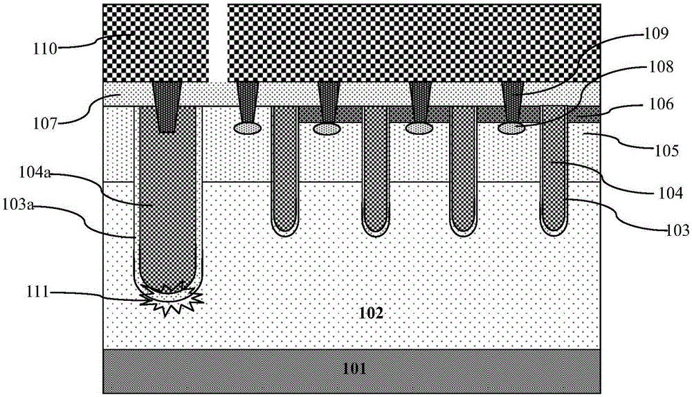
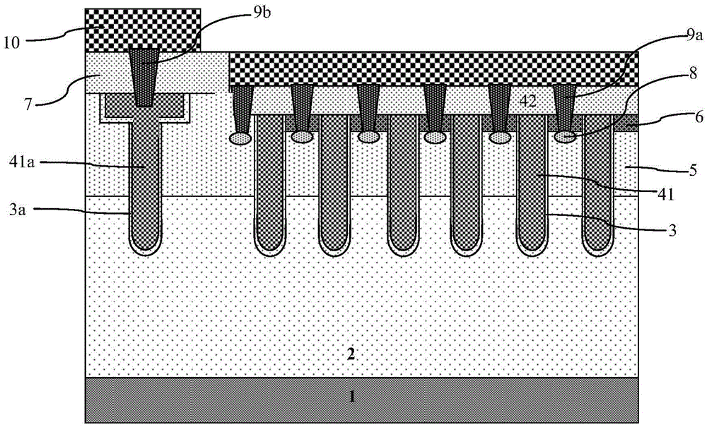
[0071] Such as figure 2 As shown, it is a schematic structural diagram of a trench-gate power transistor according to an embodiment of the present invention; the trench-gate power transistor according to an embodiment of the present invention includes:

[0072] A plurality of gate trenches formed in the device region of the semiconductor epitaxial layer 2, each of the gate trenches is arranged in parallel along the width direction, and each of the gate trenches is composed of a top trench and a bottom trench in the depth direction superimposed, the width of the top trench of each gate trench is greater than the width of the bottom trench so as to form a T-shaped structure;

[0073] A gate dielectric layer 3 is formed on the side and bottom surfaces of each gate trench, and gate polysilicon 41 is filled in the bottom trench of each gate trench, and a gate polysilicon 41 is filled in the bottom trench of each gate trench. The trench is filled with a first dielectric layer 42 . ...


PUM


Abstract

The invention discloses a trench gate power transistor. The trench gate power transistor comprises a plurality of gate trenches with T-shaped structures, gate polycrystalline silicon is filled in a bottom trench of each gate trench, and a first dielectric layer is filled in a top trench of each gate trench; source regions are formed in body junction injection layers among the gate trenches; the depth of each source region is greater than that of the top trench of the corresponding gate trench; and a trench of a first contact hole in the top of each source region is formed by etching a semiconductor epitaxial layer between the first dielectric layers of the top trenches of the corresponding two adjacent gate trenches in a self-aligning manner, so that the distance between each two gate trenches can be reduced, and the density of channels is increased. Gate leading-out trenches are also T-shaped structure, a top trench of each gate leading-out trench is relatively wide, requirements of manufacturing of contact holes are met, the value of a bottom trench of each gate leading-out trench is relatively small, so that the depth of each gate leading-out trench is relatively small, and breakdown voltage of devices can be improved. The invention further discloses a manufacturing method for the trench gate power transistor.

Description

technical field [0001] The invention relates to the field of manufacturing semiconductor integrated circuits, in particular to a trench gate power transistor; the invention also relates to a manufacturing method of the trench gate power transistor. Background technique [0002] Such as figure 1 As shown, it is a schematic structural diagram of an existing trench gate power transistor such as a power MOSFET; a semiconductor epitaxial layer such as a silicon epitaxial layer 102 is formed on a semiconductor substrate such as a silicon substrate 101, and a trench gate is formed in the device region. The trench gate is composed of gate polysilicon 104 filled in the trench, and a gate dielectric layer such as a gate oxide layer 103 is isolated between the gate polysilicon 104 and the trench side and bottom surface of the trench gate; and outside the device region Then, a structure for leading out the trench gate is formed, which is a gate lead-out structure, and the gate lead-out...

Claims


Application Information

Patent Timeline
Patent Type & Authority Applications(China)
IPC IPC(8): H01L29/78H01L29/06H01L29/423H01L21/336H01L21/768
CPCH01L21/76897H01L29/06H01L29/0611H01L29/423H01L29/4236H01L29/66477H01L29/78
Inventor 柯行飞
Owner SHANGHAI HUAHONG GRACE SEMICON MFG CORP
Why Eureka
Try Eureka