
System-in-package module assembly, system-in-package module, and electronic device

A system-level packaging and component technology, applied in circuits, inductors, electrical components, etc., can solve the problems of large thickness and size, which do not meet the thinning of portable products.

Active Publication Date: 2018-06-15
HUAWEI TECH CO LTD
View PDF5 Cites 2 Cited by
  • Summary
  • Abstract
  • Description
  • Claims
  • Application Information

AI Technical Summary

Problems solved by technology

The existing system-in-package module integrates electronic components such as control chips, resistors, and inductors on the surface of the substrate, and the inductor is placed above the chip. In terms of thickness, the thickness of the system-in-package is relatively large, which is not suitable for portability. The characteristics of thinness emphasized by type products

Method used


Image

  • System-in-package module assembly, system-in-package module, and electronic device
  • System-in-package module assembly, system-in-package module, and electronic device
  • System-in-package module assembly, system-in-package module, and electronic device

Examples


Embodiment Construction

[0023] In order to make the purpose, features and advantages of the present invention more obvious and understandable, the technical solutions in the embodiments of the present invention will be clearly and completely described below in conjunction with the accompanying drawings in the embodiments of the present invention. Obviously, the following The described embodiments are only some, not all, embodiments of the present invention. Based on the embodiments of the present invention, all other embodiments obtained by persons of ordinary skill in the art without making creative efforts belong to the protection scope of the present invention.

[0024] The terms "first", "second", "third", "fourth", etc. (if any) in the description and claims of the present invention and the above drawings are used to distinguish similar objects and not necessarily Describe a specific order or sequence. It is to be understood that the data so used are interchangeable under appropriate circumstan...


PUM


Abstract

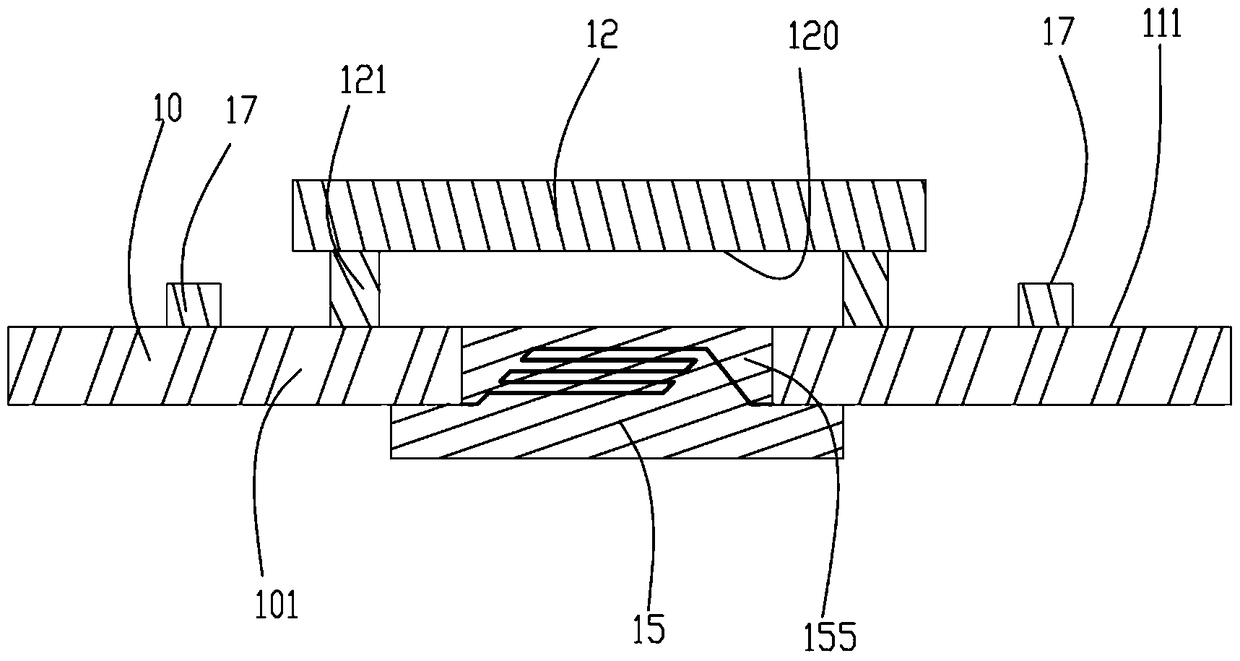
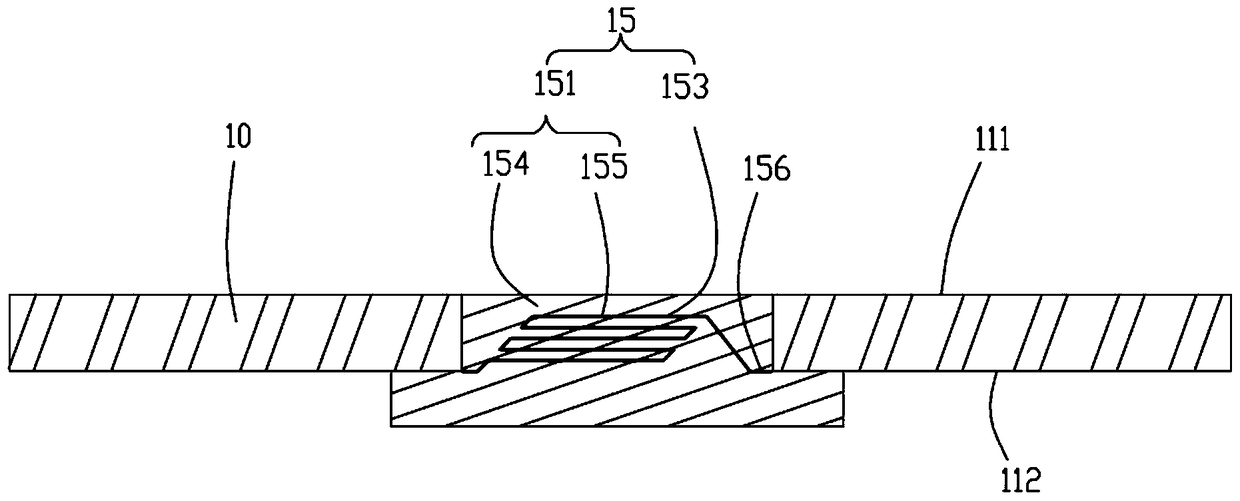
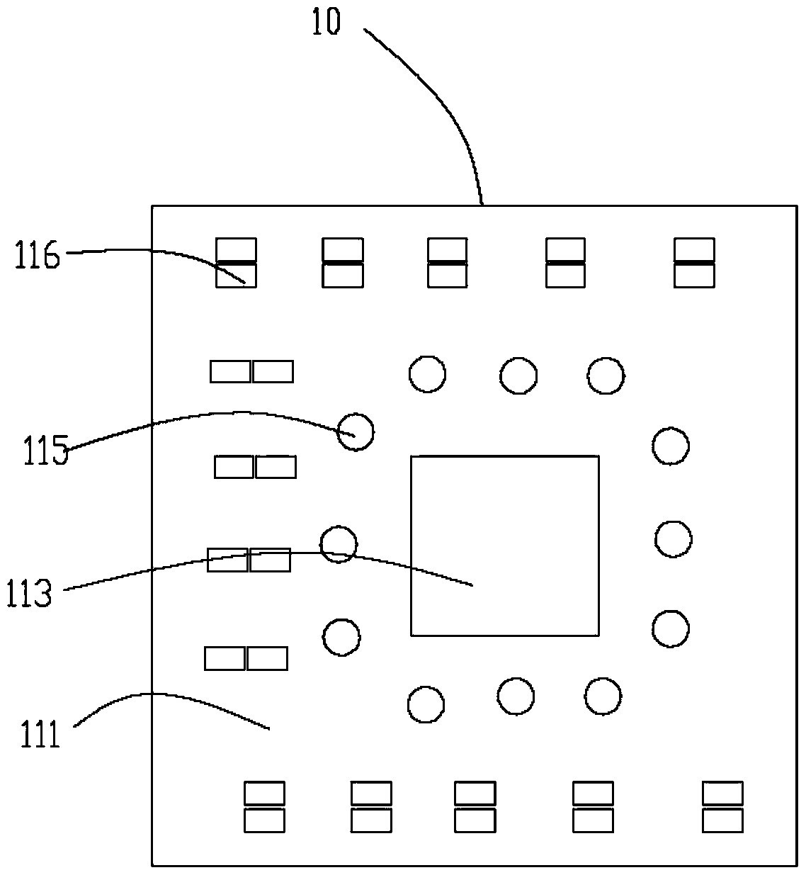
The present invention provides a system-in-package module assembly. The system-in-package module assembly includes a substrate, a chip electrically connected to the substrate, an inductor, and an electrical element. The substrate includes a first surface opposite to the first surface. The second surface and the receiving groove, the receiving groove runs through the second surface and the first surface; the inductance includes a magnetic core and an inductance coil, and the magnetic core includes a base body and a protruding part of the base body The boss on the outer surface, the outer surface of the boss protruding from the base body is attached to the second surface, the boss is accommodated in the receiving groove, and the inductance coil is embedded in the boss In the table, the chip includes a mounting surface, the chip is mounted on the first surface and the mounting surface is spaced opposite to the first surface, and the boss in the receiving groove is orthographically projected on the On the mounting surface of the chip, the electrical components are located at the periphery of the chip. The invention also provides a system-in-package module and electronic equipment.

Description

technical field [0001] The invention relates to the technical field of packaging of electronic devices, in particular to a system-in-package module assembly, a system-in-package module and electronic equipment. Background technique [0002] With the rapid growth of the portable consumer electronics market, how to accelerate the improvement of the performance of portable products in terms of thinness, lightness, small size, and low power consumption has become an important issue for system manufacturers. The system-in-package module (SiP Module System in Package or ModuleIC) with the characteristics of miniature size and low power consumption is considered to be the most suitable solution for portable products. [0003] The system-in-package module wraps a large number of electronic components, such as chips, resistors, etc., and circuits in a very small package. The biggest advantage is that it can save space and low power consumption. Wireless communication modules includi...

Claims


Application Information

Patent Timeline
Patent Type & Authority Patents(China)
IPC IPC(8): H01L25/00H01L23/488H01L23/31
CPCH01L23/31H01L23/488H01L25/00H01L2224/16225H01L2924/15311H01L2924/18161H01F17/04H01L23/49822H01L23/50H01F27/027H01F2017/048H01F3/14H01F27/24H01F27/306H01L23/492
Inventor 龚玉平侯召政王军鹤
Owner HUAWEI TECH CO LTD
Learn More