Preparation method for flexible LED array based on inorganic semiconductor material

An inorganic semiconductor and LED array technology, applied in semiconductor devices, electrical components, circuits, etc., can solve the problems of complex preparation process, and achieve the effects of good repeatability, high stability and large structure area

Active Publication Date: 2016-04-13
INST OF SEMICONDUCTORS - CHINESE ACAD OF SCI
View PDF4 Cites 8 Cited by
  • Summary
  • Abstract
  • Description
  • Claims
  • Application Information

AI Technical Summary

Problems solved by technology

Inorganic LEDs have the advantages of high energy efficiency, long life, and good stability. The preparation of inorganic flexible LEDs avoids the above problems, but Wiener processing technology has higher requirements, and the preparation process is relatively complicated.

Method used


Image

  • Preparation method for flexible LED array based on inorganic semiconductor material
  • Preparation method for flexible LED array based on inorganic semiconductor material
  • Preparation method for flexible LED array based on inorganic semiconductor material

Examples


Embodiment Construction

[0029] In order to make the object, technical solution and advantages of the present invention clearer, the present invention will be further described in detail below in conjunction with specific embodiments and with reference to the accompanying drawings.

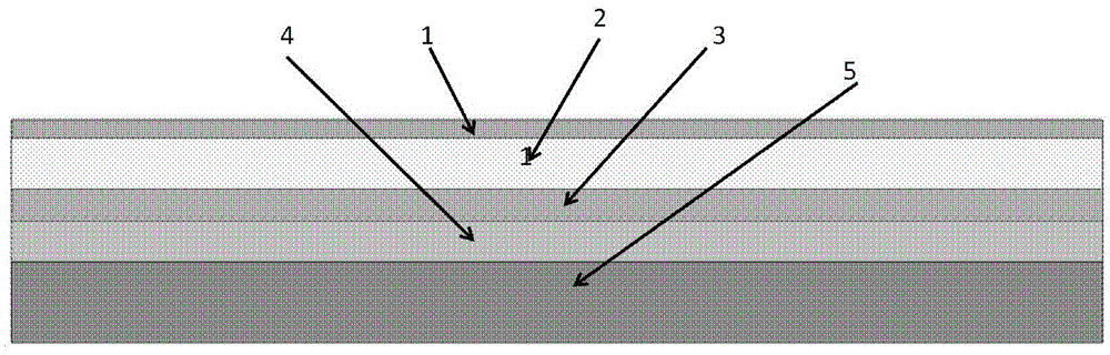
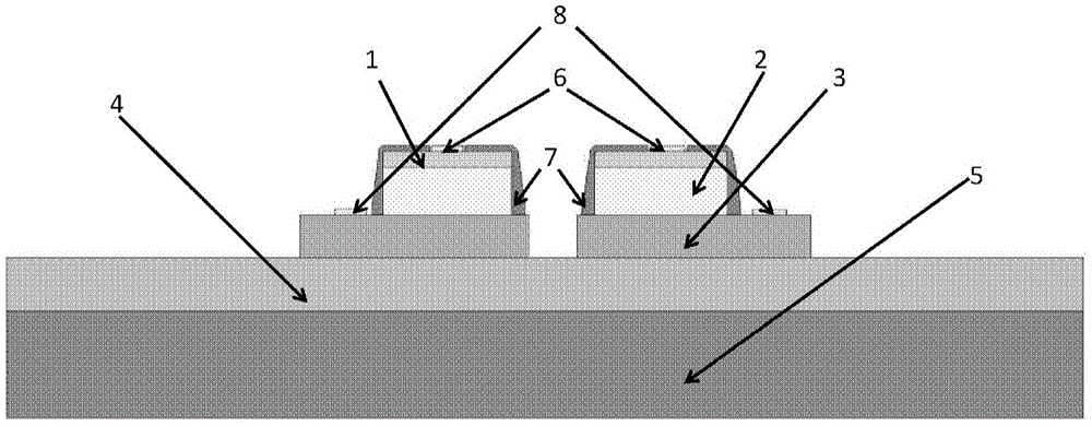
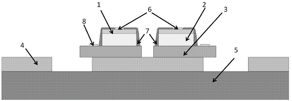
[0030] The invention proposes a method for preparing an inorganic flexible LED array, that is, using epitaxial growth technology to grow an LED epitaxial wafer with a sacrificial layer on a semiconductor substrate; cleaning the LED epitaxial wafer, and photoetching to form a ring patterned photoresist mask , etch to the lower contact layer of the LED epitaxial wafer; the side passivation layer is made by photolithography and etching process, which can effectively reduce the side leakage current caused by the side oxide layer; the patterned metal pattern is formed by ultrasonic stripping method or metal corrosion method, annealed Form ohmic contacts after alloying; photolithography forms a photoresist mask, etches the ring-...


PUM

PropertyMeasurementUnit
radiusaaaaaaaaaa
radiusaaaaaaaaaa

Abstract

The invention discloses a preparation method for a flexible LED array based on an inorganic semiconductor material. The preparation method comprises the steps of growing an LED epitaxial wafer with a sacrificial layer on a semiconductor substrate, forming annularly-patterned photoresist mask by photoetching, and etching until reaching the lower contact layer of the LED epitaxial wafer; manufacturing a side passivating layer through a photoetching process; forming a patterned metal pattern, and forming ohmic contact after performing annealing and alloying; etching an annular low table surface and exposing the sacrificial layer; etching the sacrificial layer for a certain length; spin coating a flexible polymer material; etching a polymer material covering an inner ring and the upward side of partial metal electrode to expose partial metal electrode for preparing metal interconnection; performing metal sputtering and patterning processing for preparing LED unit interconnection; spin coating the flexible polymer material; exposing the inner ring sacrificial layer; etching the residual sacrificial layer; peeling off the inorganic LED array coated with the flexible polymer; and completing the preparation for the inorganic LED array.

Description

technical field [0001] The invention belongs to the field of semiconductor optoelectronic device technology and nanometer material technology, and specifically relates to a method for preparing a flexible LED array based on an inorganic semiconductor material and an organic flexible substrate. Background technique [0002] A new type of flexible inorganic integrated device based on inorganic semiconductor materials and organic flexible substrates is a perfect combination of flexible substrates and traditional inorganic semiconductor technologies; compared with conventional organic flexible LEDs, it has the following advantages: high brightness, long life, and high stability , high efficiency; both flexible advantages; these advantages of inorganic flexible LEDs make them widely used in medical health and daily life; including: micro flexible LEDs can be made into health monitors or imaging instruments that wrap patients like blankets; As a light source for photodynamic thera...

Claims


Application Information

Patent Timeline
Patent Type & Authority Applications(China)
IPC IPC(8): H01L33/00
CPCH01L33/0093
Inventor 宋国峰李晓敏徐云江宇白霖
Owner INST OF SEMICONDUCTORS - CHINESE ACAD OF SCI
Why Eureka
Try Eureka