Real time variable parameter micro-nano optical field modulation system and interference lithography system

A modulation system, micro-nano technology, applied in microlithography exposure equipment, optics, optical components, etc., can solve the problems of complex optical settings, and achieve the effect of real-time structural parameters

Active Publication Date: 2016-04-20
SUZHOU UNIV
View PDF14 Cites 9 Cited by
  • Summary
  • Abstract
  • Description
  • Claims
  • Application Information

AI Technical Summary

Problems solved by technology

Even if a gimbal mirror is used, the period of the micro-nano structure can only be changed within a limited range, and the interferometric syst

Method used


Image

  • Real time variable parameter micro-nano optical field modulation system and interference lithography system
  • Real time variable parameter micro-nano optical field modulation system and interference lithography system
  • Real time variable parameter micro-nano optical field modulation system and interference lithography system

Examples


Embodiment 1

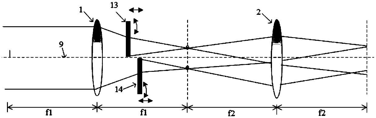
[0044] Embodiment 1: A real-time variable parameter light field modulation system based on discrete modulation of two sub-wavefronts

[0045]The real-time variable parameter micro-nano light field modulation system described in this embodiment is as follows: figure 1 As shown, in the 4F optical path system, the sub-element 13 and the sub-element 14 form a light wave modulation optical component group, and at least one of the sub-element 13 and the sub-element 14 is a binary optical element, a grating element, a holographic element or a metasurface element The sub-element 13 and the sub-element 14 can be a periodic structure or an aperiodic structure; the sub-element 13 and the sub-element 14 can be completely the same or different.

[0046] In this embodiment, if sub-element 13 is a binary optical element that eliminates 0-order light, sub-element 14 is a holographic element that eliminates 0-order light, and sub-element 13 and sub-element 14 have positive and negative first-o...

Embodiment 2

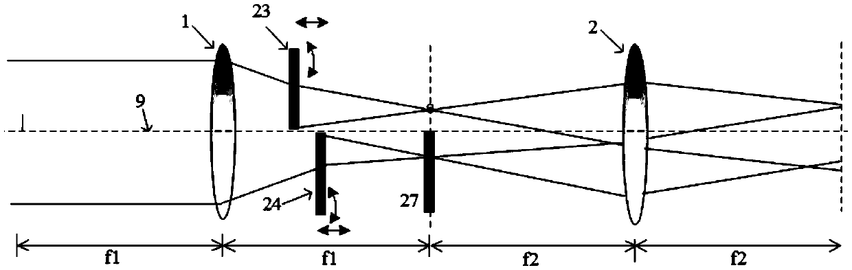
[0049] Embodiment 2: Real-time variable parameter light field modulation system with phase delay device segmented sub-wavefront modulation

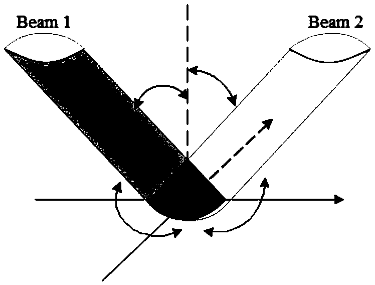
[0050] The real-time variable parameter micro-nano light field modulation system described in this embodiment is as follows: image 3 As shown, in the 4F optical system, the sub-element 23 and the sub-element 24 form a light wave modulation optical component group, and the sub-element 27 is an adjustable phase delay device. If both the sub-element 23 and the sub-element 24 are binary optical elements that only have positive and negative first-order diffracted light, then at the rear focal plane of the second lens (group), two beams of light interfere with each other, as Figure 4 As shown, and the light beam corresponding to the sub-element 24 produces different phase delays under the action of the sub-element 27 . In this embodiment, the transmitted and diffracted lights of the sub-elements 23 and 24 under the condition of vertical inci...

Embodiment 3

[0051] Embodiment 3: Real-time variable parameter light field modulation system based on three-segment sub-wavefront discrete modulation

[0052] The real-time variable parameter micro-nano light field modulation system described in this embodiment is as follows: Figure 5 As shown, in the 4F optical path system, the sub-elements 33, 34 and 38 form a light wave modulation optical component group, and the converging light wave behind the first lens (group) in the 4F optical path is divided into three sub-wavelets for modulation respectively, and the sub-elements 33, 34 and at least one of 38 is a binary optical element, a grating element, a holographic element or a metasurface element; the subelements 33, 34 and 38 can be periodic structures or non-periodic structures; the subelements 33, 34 and 38 can be identical or different.

[0053] In this embodiment, if the sub-element 33 is a grating element, the sub-element 34 is a holographic element, and the sub-element 38 is a meta...


PUM


Abstract

The application discloses a real time variable parameter micro-nano optical field modulation system and interference lithography system. The optical field modulation system comprises a light source, a 4F optical system and a light wave modulation optical component set. The 4F optical system comprises a first optical assembly and a second optical set successively arranged along an optical path; the light wave modulation optical component set is arranged between the first optical assembly and the second optical set, and generates optical field distribution with adjustable pattern and structure parameters on the back focal plane of a system through performing segmental modulation on sub wave surfaces. The system realizes separation and real time modulation of sub wave surfaces through subelements, realizes real time output of different micro-nano patterns through changing a subelement combination mode, and realizes structure parameter continuous modulation through changing subelement positions or relative positions among subelements. The system can be flexibly integrated in various lithography or microscopic systems, and realize variable parameter micro-nano structure real time write-in and adjustable micro-nano structure optical detection.

Description

technical field [0001] The invention relates to a real-time variable parameter micro-nano light field modulation system and an interference lithography system, in particular to a variable parameter light field modulation system for real-time, discrete and continuous modulation of multiple sub-wavefronts, which is applied to micro-nano structure processing, laser co-production Focal microscopy imaging, bioluminescent detection and micro / nano morphology detection. Background technique [0002] Interference lithography or holographic lithography is a technology for efficiently preparing large-scale micro-nano structures. The period of the micro-nano structures prepared by interference lithography is determined by the wavelength and angle of the interference beam (the period size is proportional to the interference wavelength, It is inversely proportional to the sine value of the interfering beam angle); its orientation is determined by the wave vector of the interfering beam; i...

Claims


Application Information

Patent Timeline
IPC IPC(8): G02B27/00G03F7/20
CPCG02B27/00G03F7/7045
Inventor 叶燕许峰川魏国军许宜申浦东林陈林森
Owner SUZHOU UNIV
Why Eureka
Try Eureka