Surface enhanced Raman scattering optical flow chip and cleaning method thereof

A surface-enhanced Raman and optical flow technology, applied in the field of optofluidic detection, can solve the problems of limiting the sensitivity and repeatability of optical fiber substrates, limiting the application of SERS detection, limiting miniaturization and integration, and achieving trace detection , reusable, and reproducible effects

Active Publication Date: 2020-06-16
SOUTH CHINA NORMAL UNIVERSITY
View PDF7 Cites 6 Cited by
  • Summary
  • Abstract
  • Description
  • Claims
  • Application Information

AI Technical Summary

Problems solved by technology

Although these SERS substrates have become relatively mature and are common tools for enhancing Raman signals, their high preparation costs and complicated processes require specialized equipment and specialized operations.
Moreover, the relatively large substrate area limits their miniaturization and integration, which greatly limits the further application of SERS detection in trace liquid detection and real-time detection.
Optical fiber sensing has the advantages of simple preparation, small size, and flexible operation, but it can only detect SERS signals in high-concentration solutions and is difficult to self-clean, which limits the sensitivity and repeatability of optical fiber substrates.

Method used


Image

  • Surface enhanced Raman scattering optical flow chip and cleaning method thereof
  • Surface enhanced Raman scattering optical flow chip and cleaning method thereof
  • Surface enhanced Raman scattering optical flow chip and cleaning method thereof

Examples


Embodiment 1

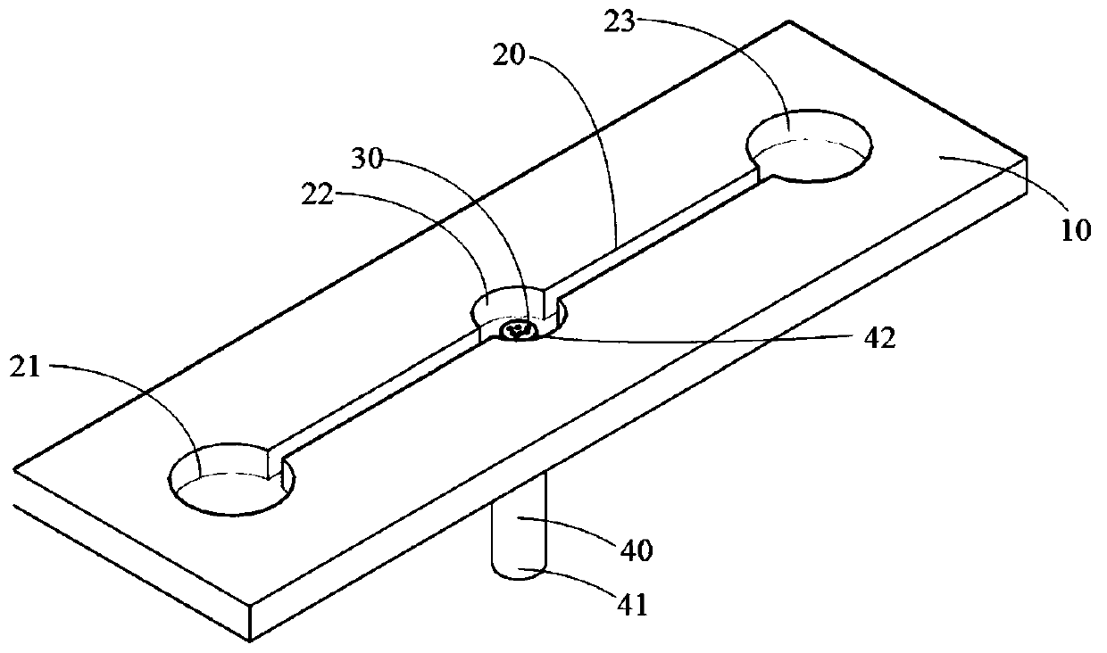
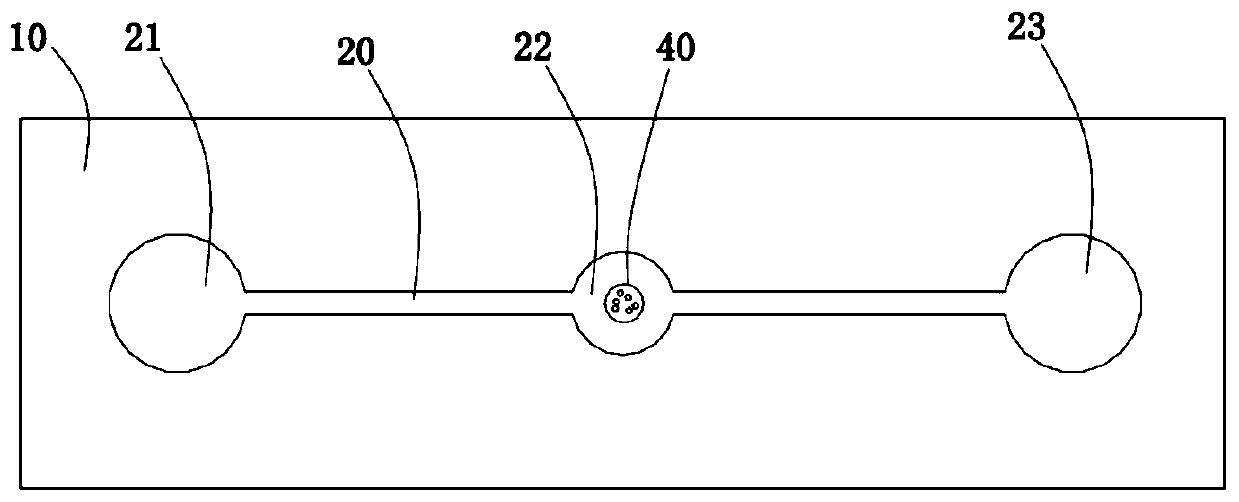
[0056] like figure 1 As shown, the surface-enhanced Raman scattering optical flow chip according to the first embodiment of the present invention includes a substrate 10 , a microfluidic channel 20 , a metal nano-island substrate 30 and an optical fiber 40 . The microfluidic channel 20 is disposed in the substrate 10, and the microfluidic channel 20 is used to accommodate the solution to be detected; the optical fiber 40 includes an optical signal input end 41 and an excitation end 42, and the optical signal input end 41 is used to connect the optical signal, and the excitation end 42 is arranged in the microfluidic channel 20 . The metal nano-island substrate 30 is formed on the end face of the excitation end 42 , wherein the metal nano-island substrate 30 is used to generate surface plasmon resonance under the excitation of an external laser, so as to adsorb the substance molecules in the solution to be detected. After the detection is completed, the optical signal is conne...

Embodiment 2

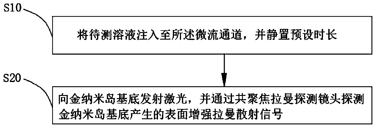
[0066] like image 3 As shown, according to the second embodiment of the present invention, the detection method of the surface-enhanced Raman scattering optical flow chip includes the following steps:

[0067] Step S10: inject the solution to be tested into the microfluidic channel 20, and let it stand for a preset period of time.

[0068] Specifically, the solution to be detected is injected from the injection port 21 using a syringe pump, so that the solution to be detected fills the microfluidic channel. It was left to stand for one minute so that the substance molecules were completely adsorbed on the metal nano-island substrate 30 . The solution to be detected is a solution containing the substance to be detected. In order to make the detection accuracy more sensitive, it is recommended to use pure substance or its aqueous solution as the solvent, and in order to make the substance molecules to be detected have better adsorption on the SERS substrate , Exemplarily, the...

Embodiment 3

[0085] like Figure 7 As shown, the cleaning method of the surface-enhanced Raman scattering optical flow chip according to the third embodiment of the present invention includes the following steps:

[0086] Step S100: Pour deionized water into the microfluidic channel 20, and make the deionized water submerge the metal nano-island substrate.

[0087] Specifically, a syringe pump is used to inject deionized water from the inlet, and the remaining solution in the channel after detection is taken out of the channel. When the chip is in a cleaning state, the cleaning liquid is deionized water.

[0088] Step S200 : connecting the optical signal to the optical signal input end 41 , turning off the optical signal after a predetermined period of time, and removing the deionized water in the microfluidic channel 20 .

[0089] Specifically, when the optical fiber 40 passes light, because the metal nano-island substrate 30 has a good photothermal effect, heat will be generated on the ...


PUM

PropertyMeasurementUnit
thicknessaaaaaaaaaa
poweraaaaaaaaaa
wavelengthaaaaaaaaaa

Abstract

The invention discloses a surface enhanced Raman scattering optical flow chip and a cleaning method thereof. The optical flow chip includes a substrate, a microfluidic channel which is arranged in thesubstrate and is used for accommodating a to-be-detected solution, an optical fiber which comprises an optical signal input end used for accessing an optical signal and an excitation end arranged inthe microfluidic channel, and a metal nano island substrate which is formed on the end surface of the excitation end and is used for generating surface plasma resonance under the excitation of external laser so as to adsorb substance molecules in the to-be-detected solution. The cleaning method comprises the following steps: introducing deionized water into the microfluidic channel, and enabling the deionized water to submerge the metal nano island substrate; and accessing an optical signal into the optical signal input end, closing the optical signal after a preset duration, and removing thedeionized water in the microfluidic channel. The chip is simple in structure, small in size, easy and convenient to manufacture, can detect low-concentration substances to be detected, can be rapidlycleaned and has improved reusability.

Description

technical field [0001] The invention belongs to the technical field of optofluidic detection, and in particular relates to an optofluidic chip with surface-enhanced Raman scattering and a cleaning method thereof. Background technique [0002] Surface-Enhanced Raman Scattering (SERS), as a common and advanced material detection method, plays a vital role in the fields of chemistry, biomedicine and environmental protection. Since the SERS intensity is related to the surface plasmon resonance of the metal nanostructures, and strongly depends on the geometry of the metal nanostructures. Therefore, common SERS substrates are mainly prepared by chemical adsorption, laser-induced deposition, in-situ reduction, and photolithography to prepare metal nanoparticles / structures. Although these SERS substrates have become relatively mature and common tools for enhancing Raman signals, their high fabrication costs and complex processes require specialized equipment and specialized operati...

Claims


Application Information

Patent Timeline
Patent Type & Authority Applications(China)
IPC IPC(8): B01L3/00G01N21/65
CPCB01L3/50273B01L3/502715B01L3/5027G01N21/658B01L2300/0654B01L2300/168B01L2400/0433B01L2400/0415
Inventor 邢晓波刘绍静李宗宝徐宇吴家隐郑志东陈伊琳
Owner SOUTH CHINA NORMAL UNIVERSITY
Why Eureka
Try Eureka