Semiconductor capacitor based on through-silicon via technology and manufacturing method and packaging structure thereof

A technology for semiconductors and capacitors, applied in the field of semiconductor capacitors and their manufacturing based on through-silicon via technology, can solve the problems of large volume, incompatibility of semiconductor processes, and increase in chip cost, so as to increase electrode area, reduce parasitic effects, and improve capacitance. effect of value

Inactive Publication Date: 2016-04-20
TIANJIN UNIV
View PDF5 Cites 12 Cited by
  • Summary
  • Abstract
  • Description
  • Claims
  • Application Information

AI Technical Summary

Problems solved by technology

However, the capacitance value per unit area of ​​this type of capacitor is low, such as the MIM capacitor is about 2fF / μm 2 ,, Therefore, if you want to obtain a capacitor with a larger capacity (such as above 10PF), you need to occupy a very large chip area, which increases the cost of the chip
For example, chip capacitors in discrete devices often use a multi-layer interdigitated electrode structure, which can have a large capacitance, but is large in size, incompatible with semiconductor processes, and inconvenient for miniaturized packaging with integrated circuit chips.

Method used


Image

  • Semiconductor capacitor based on through-silicon via technology and manufacturing method and packaging structure thereof
  • Semiconductor capacitor based on through-silicon via technology and manufacturing method and packaging structure thereof
  • Semiconductor capacitor based on through-silicon via technology and manufacturing method and packaging structure thereof

Examples


Embodiment Construction

[0048] The technical solution of the present invention will be described in further detail below in conjunction with the accompanying drawings and specific embodiments.

[0049] The invention discloses an embodiment of a manufacturing method of a semiconductor capacitor, such as Figure 1-Figure 9 As shown, the following steps are included in sequence:

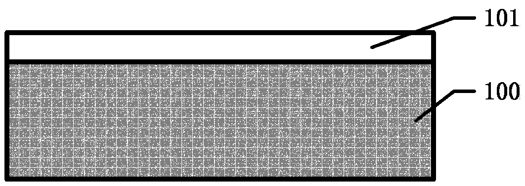
[0050] In the first step, a layer of insulating layer 101 is deposited on the substrate 100, such as figure 1 shown;

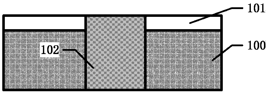
[0051] The second step is to etch a via hole through the substrate 100 and the insulating layer 101, and then fill the bottom electrode metal column 102 in the via hole, such as figure 2 shown;

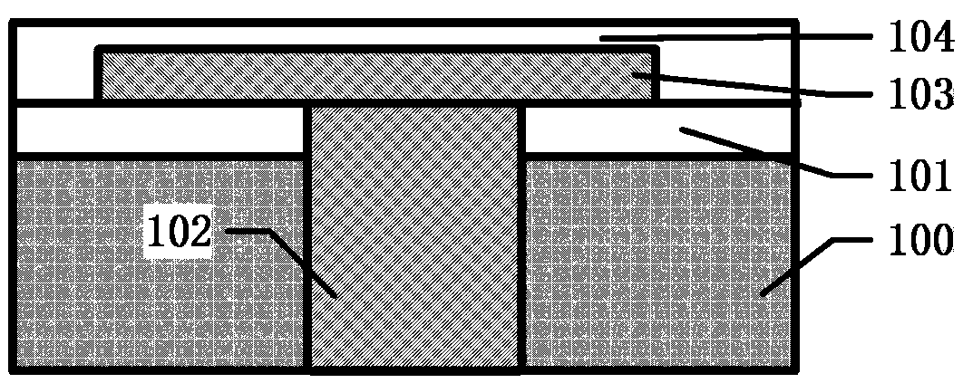
[0052] In the third step, the first metal layer 103 and the first dielectric layer 104 are successively deposited on the surface of the insulating layer 101, such as image 3 shown;

[0053] The fourth step is to form the second metal layer 105 and the second dielectric layer 106 based on the successive deposit...


PUM


Abstract

The invention discloses a semiconductor capacitor based on the through-silicon via technology and a manufacturing method and a packaging structure thereof. The semiconductor capacitor comprises metal-insulation dielectric layer laminated structures formed by multiple metal layers and insulation dielectric layers in a repeated mode, the metal layers in even layers are electrically connected, and the metal layers in odd layers are electrically connected; each laminated structure is provided with a substrate, and a bottom electrode metal column penetrates through each substrate. Compared with the prior art, the electrode area of the capacitor formed in a laminated mode is increased on the condition that the occupation area is not enlarged, so that the capacitance value is improved, and the cost is saved; two electrodes of the metal-insulation-metal capacitor can be guided by metal above the substrates and metal below the substrates respectively, the capacitor can be electrically connected with different external circuits (such as an integrated circuit chip and a PCB) through the 3D packaging technology, miniaturization encapsulation can be achieved, and the parasitic effect is reduced.

Description

technical field [0001] The invention relates to the technical field of manufacturing semiconductor capacitors, in particular to a semiconductor capacitor based on through-silicon via technology and a manufacturing method thereof. Background technique [0002] Capacitive components are often used in integrated circuits as electronic passive devices, with functions such as energy storage, filtering, and DC blocking, and are one of the widely used components. At present, common capacitor structures in the semiconductor process include metal oxide semiconductor (MOS) capacitors, PN junction capacitors, and metal-insulator-metal (MIM) capacitors. However, the capacitance value per unit area of ​​this type of capacitor is low, such as the MIM capacitor is about 2fF / μm 2 ,, Therefore, if you want to obtain a capacitor with a larger capacity (such as above 10PF), you need to occupy a very large chip area, which increases the cost of the chip. For example, chip capacitors in discre...

Claims


Application Information

Patent Timeline
Patent Type & Authority Applications(China)
IPC IPC(8): H01L23/64H01L23/48H01L23/488
CPCH01L28/40H01L23/481H01L23/488H01L28/91
Inventor 赵毅强胡凯赵公元刘沈丰
Owner TIANJIN UNIV
Why Eureka
Try Eureka