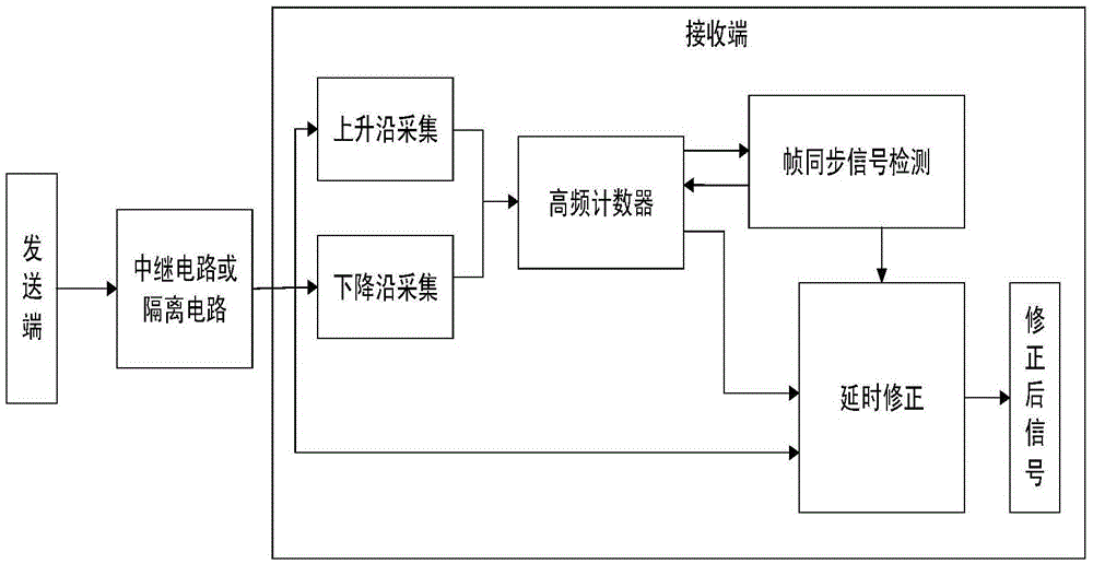
Digital signal edge delay correction system and method
A digital signal and edge technology, applied in the field of digital signal edge delay correction system, can solve the problems of signal distortion, speed up the rising edge speed, increase the charging speed of triode, etc., to repair distortion, reduce complexity, and reduce hardware transmission speed requirements Effect
- Summary
- Abstract
- Description
- Claims
- Application Information
AI Technical Summary
Problems solved by technology
Method used
Image
Examples
Embodiment 1
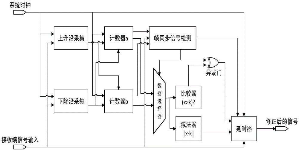
[0043] Such as figure 2 As shown, the digital signal edge delay correction system of this embodiment adopts FPGA as the main control chip of the receiving end, and the FPGA includes a rising edge acquisition module, a falling edge acquisition module, a counter a, a timer b, and a frame synchronization signal detection module, Data selector, XOR gate, comparator, subtractor, delayer.
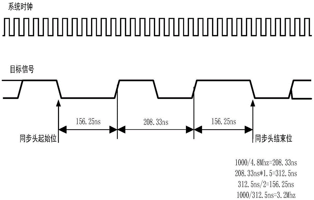
[0044] The system uses non-return-to-zero code to transmit data, the level change represents 1, and the level remains unchanged represents 0. The system clock adopts 38.4MHz, the signal frequency is 4.8MHz (bit rate 9.6Mbps), and the pulse width is 1.5 times as stated in the transmission protocol. The pulse corresponds to a frequency of 3.2MHz (1 / 4.8MHz*1.5=1 / 3.2MHz). The frame synchronization header of the data consists of a 3.2MHz half-wave (1 / 3.2MHz*1 / 2*1000=156.25ns), a 4.8MHz full-wave (1 / 4.8MHz*1000=208.33ns), a 3.2MHz A special sequence composed of half waves, the receiving end recogniz...
Embodiment 2
[0053] Such as figure 2 As shown, the digital signal edge delay correction system of this embodiment adopts FPGA as the main control chip of the receiving end, and the FPGA includes a rising edge acquisition module, a falling edge acquisition module, a counter a, a timer b, and a frame synchronization signal detection module, Data selector, XOR gate, comparator, subtractor, delayer.
[0054] The system uses non-return-to-zero code to transmit data, the level change represents 1, and the level remains unchanged represents 0. The system clock adopts 153.6MHz, the signal frequency is 4.8MHz (bit rate 9.6Mbps), and the pulse width is 1.5 times as stated in the transmission protocol. The pulse corresponds to a frequency of 3.2MHz (1 / 4.8MHz*1.5=1 / 3.2MHz). The frame synchronization header of the data consists of a 3.2MHz half-wave (1 / 3.2MHz*1 / 2*1000=156.25ns), a 4.8MHz full-wave (1 / 4.8MHz*1000=208.33ns), a 3.2MHz A special sequence composed of half waves, the receiving end recogni...
Embodiment 3
[0063] Such as figure 2 As shown, the digital signal edge delay correction system of this embodiment adopts FPGA as the main control chip of the receiving end, and the FPGA includes a rising edge acquisition module, a falling edge acquisition module, a counter a, a timer b, and a frame synchronization signal detection module, Data selector, XOR gate, comparator, subtractor, delayer.
[0064] The system uses non-return-to-zero code to transmit data, the level change represents 1, and the level remains unchanged represents 0. The system clock adopts 38.4MHz, the signal frequency is 4.8MHz (bit rate 9.6Mbps), and the transmission protocol is 0.5 times the pulse width. The pulse corresponds to a frequency of 9.6MHz (1 / 4.8MHz*0.5=1 / 9.6MHz). The frame synchronization header of the data consists of a 9.6MHz half-wave (1 / 9.6MHz*1 / 2*1000=52.08ns), a 4.8MHz full-wave (1 / 4.8MHz*1000=208.33ns), a 9.6MHz A special sequence composed of half waves, the receiving end recognizes the identit...
PUM
 Abstract
Description
Claims
Application Information


