A short-circuited anode lateral insulated gate bipolar transistor
An anode and lateral technology, applied in the direction of circuits, semiconductor devices, electrical components, etc., can solve problems that affect the stability of power electronic systems and devices cannot be turned on normally, so as to improve the off-state characteristics and anti-latch-up ability, and suppress the snapback phenomenon Effect
- Summary
- Abstract
- Description
- Claims
- Application Information
AI Technical Summary
Problems solved by technology
Method used
Image

Examples
Embodiment 1
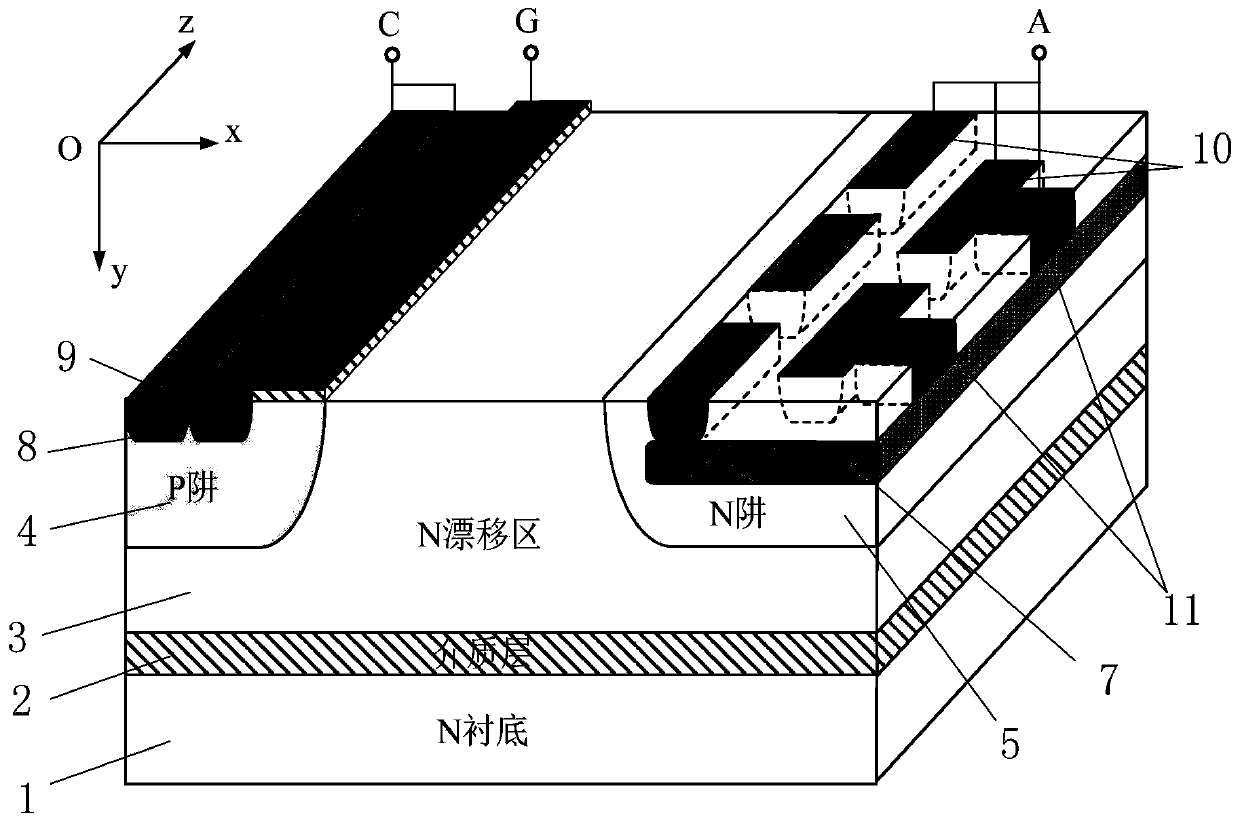
[0029] Such as figure 2 As shown, it includes an N-type substrate 1, a dielectric layer 2 located on the upper surface of the N-type substrate, and an N-type drift region 3 located on the upper surface of the dielectric layer 2; the upper side of the N-type drift region 3 has a P-type well region 4, the other side has an N-type well region 5; the upper layer of the P-type well region 4 has a P+ body contact region 8 and an N+ cathode region 9, and the P+ body contact region 8 and N+ cathode region 9 are juxtaposed along the lateral direction of the device set, and the N+ cathode region 9 is located on the side close to the N-type well region 5; the upper surface of the P-type well region 4 between the N+ cathode region 9 and the N-type drift region 3 has a gate structure; it is characterized in that, The upper layer of the N-type well region 5 has a P+ anode region 10 and an N+ anode region 11, and the P+ anode region 10 is located on a side close to the P-type well region 4;...
Embodiment 2
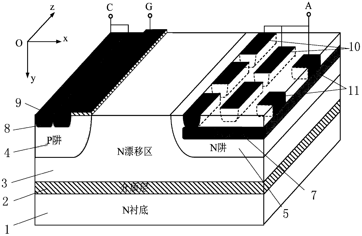
[0034] Such as image 3 As shown, the structure of this example is basically the same as that of the embodiment, except that in this example, the N+ anode region 11 is separated from a row of adjacent P+ anode subregions.
[0035] The principles and beneficial effects of this embodiment are the same as those of Embodiment 1, but another implementation manner is provided.
Embodiment 3
[0037] Such as Figure 4 As shown, the structure of this example is basically the same as that of Example 2. The difference is that in this example, the P+ anode region 10 includes three columns, which are respectively the first row of P+ anode subregions, the second row of P+ anode subregions and the third row of P+ anode subregions. Row P+ anode sub-region; the distance between the first row P+ anode sub-region and the second row P+ anode sub-region is m1, the distance between the second row P+ anode sub-region and the third row P+ anode sub-region The pitch is m2; the first row of P+ anode sub-regions is divided into two sections along the longitudinal direction of the device, which are respectively the first row of the first segment of the P+ anode sub-region and the first row of the second segment of the P+ anode sub-region, the first The first column of the P+ anode sub-region is located on one side of the device along the longitudinal direction of the device, the second...
PUM
 Abstract
Description
Claims
Application Information
 - R&D
- Intellectual Property
- Life Sciences
- Materials
- Tech Scout
- Unparalleled Data Quality
- Higher Quality Content
- 60% Fewer Hallucinations
Browse by: Latest US Patents, China's latest patents, Technical Efficacy Thesaurus, Application Domain, Technology Topic, Popular Technical Reports.
© 2025 PatSnap. All rights reserved.Legal|Privacy policy|Modern Slavery Act Transparency Statement|Sitemap|About US| Contact US: help@patsnap.com