Supercharge Your Innovation With Domain-Expert AI Agents!

Welding method of SMD electrolytic capacitor

A technology of electrolytic capacitors and welding methods, which is applied in the direction of assembling printed circuits, electrical components, and printed circuits with electrical components. Effect of Mounting Cost

Inactive Publication Date: 2016-05-04
SHENZHEN SUNTAK MULTILAYER PCB
View PDF6 Cites 0 Cited by
  • Summary
  • Abstract
  • Description
  • Claims
  • Application Information

AI Technical Summary

Problems solved by technology

[0004] For this reason, the technical problem to be solved by the present invention is that in the welding process of chip electrolytic capacitors in the prior art, the shape and size of the opening of the stencil are the same as that of the pad, and the solder melts during welding, and the capacitor easily causes the solder to overflow under the action of gravity, which is wasteful. It is easy to cause short circuit of solder joints, so a welding method for electrolytic capacitors that prevents solder overflow, avoids short circuit of solder joints and saves manufacturing cost is proposed

Method used


Image

  • Welding method of SMD electrolytic capacitor
  • Welding method of SMD electrolytic capacitor

Examples


Embodiment

[0029] The present embodiment provides a welding method for chip electrolytic capacitors, which includes the following steps:

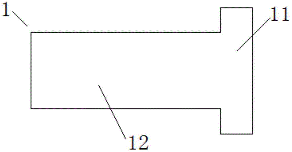
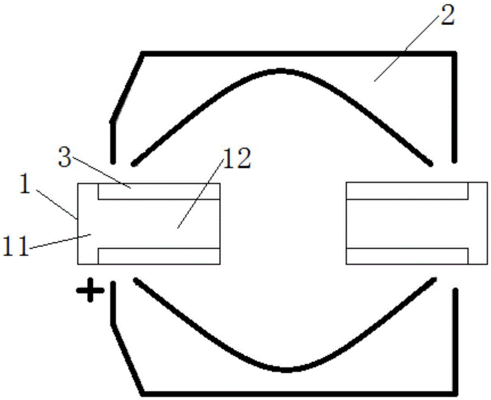
[0030] S1, making a steel mesh, the opening 1 of the welding pad on the steel mesh is T-shaped, and consists of a first rectangular part 11 and a second rectangular part 12 that are vertically connected to each other, such as Figure 1-2 As shown, the length of the first rectangular part 11 of the pad opening 1 is 70-90mil, and the width is 20-30mil; the length of the second rectangular part 12 is 110-130mil, and the width is 40-60mil. In this embodiment , the body diameter of the chip electrolytic capacitor 2 is 8 mm, the length of the first rectangular part 11 of the pad opening 1 is 80 mil, and the width is 20 mil; the length of the second rectangular part 12 is 120 mil, and the width is 48 mil. The short side of the second rectangular part 12 is arranged perpendicular to the long side of the first rectangular part 11, and the short side of the sec...


PUM


Abstract

The invention discloses a welding method of an SMD electrolytic capacitor. The welding method includes the following steps that: S1, a steel net is produced, the section of a pad opening of the steel net is T-shaped and is composed of a first rectangular portion and a second rectangular portion which are vertically communicated with each other; S2, solder printing is performed by adopting the steel net obtained in the step 1, and the pad opening is arranged in a manner that the pad opening is corresponding to the pad of the SMD electrolytic capacitor; S3, surface mounting is carried out: the SMD electrolytic capacitor is mounted on solder in a surface-mount manner; and S4, reflow soldering is carried out: the SMD electrolytic capacitor is welded on a printed circuit board. According to the method of the invention, the section of the pad opening of the steel net is designed to a T-shaped opening the size of which is smaller than that of the pad of the SMD electrolytic capacitor, and therefore, the area of the pad opening can be decreased, space can be reserved for the overflow of soldering tin, the probability of the overflow of the soldering tin can be reduced, welding points can be prevented from being short-circuited, welding yield can be improved, the consumption of the solder can be decreased, and surface-mounting cost can be decreased.

Description

technical field [0001] The invention belongs to the technical field of printed circuit board production, and in particular relates to a welding method for patch electrolytic capacitors. Background technique [0002] The printed circuit board (Printed Circuit Board, referred to as PCB) is an important electronic component, a support for electronic components, and an electrical connection carrier for electronic components, and can realize automatic insertion or placement of electronic components, automatic soldering, automatic Testing ensures the quality of electronic equipment, improves labor productivity, reduces costs, and facilitates maintenance. [0003] With the development of the electronics industry, electronic products are becoming more and more miniaturized and integrated, and the PCB structure is also required to become more and more complex, so that the proportion of SMD components on the circuit board is increasing. Among them, SMD electrolytic capacitors are used...

Claims


Application Information

Patent Timeline
IPC IPC(8): H05K3/34
CPCH05K3/341H05K2201/10015
Inventor 齐军刘德良杨林吴和燕董振超曾光
Owner SHENZHEN SUNTAK MULTILAYER PCB
Features
  • R&D
  • Intellectual Property
  • Life Sciences
  • Materials
  • Tech Scout
  • Unparalleled Data Quality
  • Higher Quality Content
  • 60% Fewer Hallucinations
Learn More