Formation method of semiconductor device

A semiconductor and device technology, applied in the field of semiconductor device formation, can solve the problems that the second wafer 20 is prone to cracking, affecting the performance and yield of MEMS devices, etc.

Active Publication Date: 2016-05-11
SEMICON MFG INT (SHANGHAI) CORP
View PDF5 Cites 8 Cited by
  • Summary
  • Abstract
  • Description
  • Claims
  • Application Information

AI Technical Summary

Problems solved by technology

[0009] but refer to Figure 4 As shown, in the formation process of the above-mentioned MEMS device, the second wafer 20 is prone to fragmen

Method used


Image

  • Formation method of semiconductor device
  • Formation method of semiconductor device
  • Formation method of semiconductor device

Examples


Embodiment Construction

[0054] As mentioned in the background, in the existing manufacturing process of MEMS devices, wafer fragmentation often occurs, thereby affecting the performance and yield of MEMS devices. Analyze its reasons:

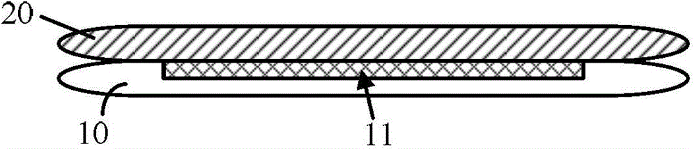
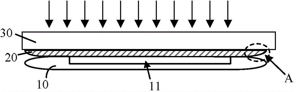
[0055] In the field of semiconductor manufacturing, existing wafers are mostly made of brittle materials such as silicon and germanium. In order to prevent wafers from being damaged due to bumping, the side walls of existing wafers are mostly arc-shaped curved surface structures. combined reference figure 2 with Figure 4 , in the preparation of MEMS devices, when the second wafer 20 is planarized, the edge of the second wafer 20 is in a suspended state not supported by the first wafer 10 (as shown in part A), so chemical During the grinding process of the second wafer 20 by mechanical grinding and other planarization techniques, the edge of the second wafer 20 is easily broken due to pressure, and cracks 21 with a large area appear on the edge of the second wafer 2...


PUM


Abstract

The invention provides a formation method of a semiconductor device. The formation method is characterized by comprising the following steps: providing a first wafer and a second wafer, and enabling the first wafer to be in bonding connection with the second wafer; performing edge-trimming treatment on the second wafer so as to remove the arc curved surface structure on the periphery of the second wafer; performing primary attrition treatment on the back surface of the second wafer so as to reduce partial thickness; fixing a third wafer on the back surface of the second wafer subjected to primary attrition treatment; after performing edge-trimming treatment on the second wafer to remove the arc curved surface structure on the side wall of the second wafer, preventing a suspended structure from being formed at the edge of the second wafer during the primary attrition treatment on the back surface of the second wafer, thereby solving the problem that the second wafer, when pressed during attrition, cracks at the edge due to the suspended structure formed at the edge, and improving the quality of the second wafer after attrition as well as the performance and the finished product rate of semiconductor devices formed subsequently.

Description

technical field [0001] The invention relates to the field of semiconductors, in particular to a method for forming a semiconductor device. Background technique [0002] Micro-Electro-Mechanical-Systems (MEMS for short) is a micro-system that uses micro-fabrication technology to integrate sensors, actuators, and processing control circuits on a chip. [0003] Some MEMS highly integrated components include a cavity and a cantilever beam located in the cavity and suspended at one end. During use, the cantilever beam vibrates up and down and electrically responds to the element in the semiconductor substrate to transmit signals. [0004] Existing MEMS device fabrication processes include: [0005] refer to figure 1 As shown, a first wafer 10 is first formed (semiconductor elements such as transistors are formed in the first wafer 10), and after a groove 11 is formed in the first wafer 10, the first wafer 10 is covered with a second wafer 20, and the second wafer 20 can cover...

Claims


Application Information

Patent Timeline
IPC IPC(8): B81C3/00B81C1/00
Inventor 徐伟刘国安
Owner SEMICON MFG INT (SHANGHAI) CORP
Why Eureka
Try Eureka