Photoresist removal method and rework method of photolithography process

A photolithography process and photoresist technology, which is applied in the direction of photosensitive material processing, photoplate making process coating equipment, electrical components, etc., can solve the problems of product yield reduction, inability to remove particle defects, wafer scrapping, etc., and achieve improvement Yield, the effect of reducing the probability of pattern distortion defects

Active Publication Date: 2019-11-05
SEMICON MFG INT (SHANGHAI) CORP
View PDF2 Cites 0 Cited by
  • Summary
  • Abstract
  • Description
  • Claims
  • Application Information

AI Technical Summary

Problems solved by technology

[0005] In view of the above-mentioned shortcoming of the prior art, the purpose of the present invention is to provide a method for removing photoresist and a rework method for photolithography, which are used to solve the problem that the existing methods cannot remove the particles in the photoresist on the surface of the wafer. Defects are completely removed, and then pattern distortion defects are generated in the etching process, which reduces the yield of the product and even makes the entire wafer scrapped

Method used


Image

  • Photoresist removal method and rework method of photolithography process
  • Photoresist removal method and rework method of photolithography process
  • Photoresist removal method and rework method of photolithography process

Examples


Embodiment Construction

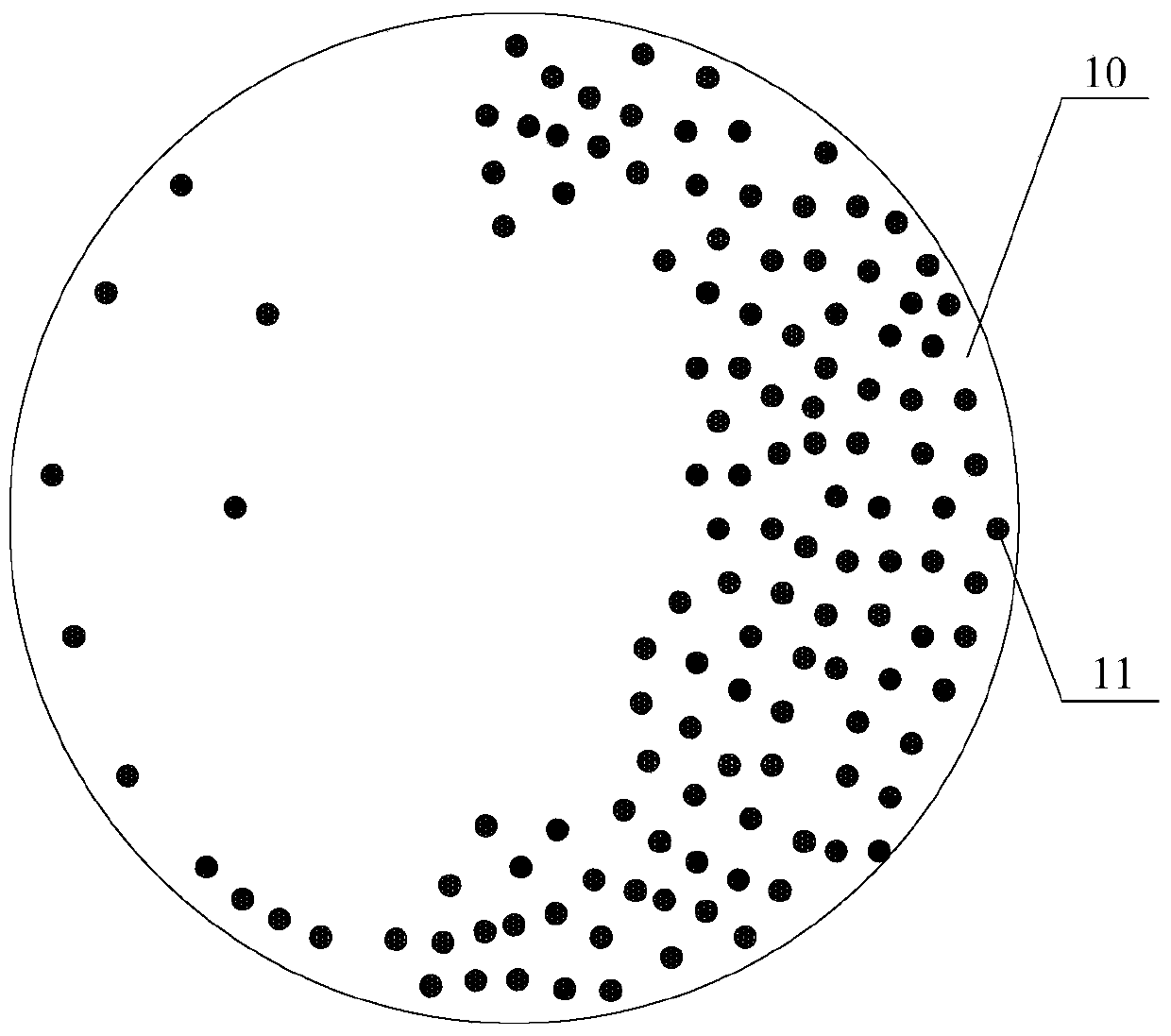
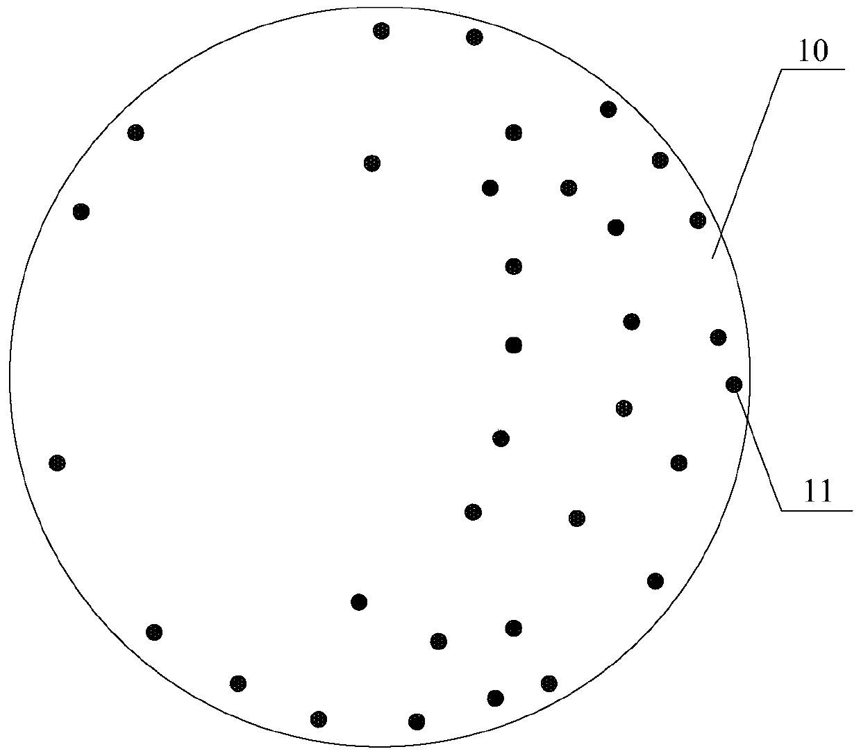
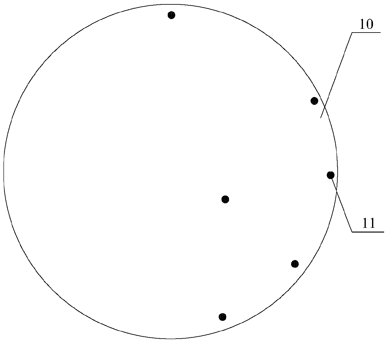
[0040] The following describes the implementation of the present invention through specific specific examples. Those skilled in the art can easily understand other advantages and effects of the present invention from the content disclosed in this specification. The present invention can also be implemented or applied through other different specific embodiments, and various details in this specification can also be modified or changed based on different viewpoints and applications without departing from the spirit of the present invention.

[0041] See Figure 2 to Figure 4 . It should be noted that the illustrations provided in this embodiment only illustrate the basic idea of ​​the present invention in a schematic manner, although the figures only show components related to the present invention instead of the number, shape, and shape of the components in actual implementation. For size drawing, the type, quantity, and proportion of each component can be changed at will during ...


PUM


Abstract

The invention provides a photoresist removal method and a photoetching process reworking method. The photoresist removal method comprises rotating a wafer at a high rate, dissolving partial-thickness of a photoresist layer on the wafer surface through a photoresist diluent RRC, simultaneously, carrying away large particles in the photoresist layer through the photoresist diluent RRC, removing the residual photoresist layer through oxygen plasmas and washing the surface of the wafer through a wet washing method. The photoresist removal method can effectively and completely remove particle defects in the photoresist, reduces graphic distortion defect probability of the later etching technology and improves a product yield.

Description

Technical field [0001] The invention belongs to the manufacturing field of semiconductor devices, and relates to a photoresist removal method and a photoetching process rework method. Background technique [0002] In semiconductor device manufacturing technology, a photolithography process is usually used to transfer the mask pattern on the mask to the photoresist layer on the wafer surface. Usually the basic process of photolithography includes the steps of coating, exposing and developing. The purpose of gluing is to create a thin, uniform and defect-free photomask layer on the surface of the wafer; the purpose of exposure is to transfer the mask pattern to the photoresist layer using the exposure light source; development is to pattern the photoresist layer, The exposed or unexposed areas of the photoresist layer are removed, thereby forming a patterned photoresist layer on the wafer surface. Then, the wafer is etched under the mask of the patterned photoresist layer, and th...

Claims


Application Information

Patent Timeline
Patent Type & Authority Patents(China)
IPC IPC(8): G03F7/42G03F7/16H01L21/02H01L21/311
Inventor 袁文勋陈杰
Owner SEMICON MFG INT (SHANGHAI) CORP
Why Eureka
Try Eureka