A Schottky diode and its manufacturing method
A Schottky diode and bowl-shaped technology, applied in the field of Schottky diodes and their fabrication, can solve the problems of inaccurate size control at the widest point of the P-well, inability to reduce VF, and device stability degradation, etc. The effect of junction process, electron capture ability enhancement, VF reduction
- Summary
- Abstract
- Description
- Claims
- Application Information
AI Technical Summary
Problems solved by technology
Method used
Image
Examples
Embodiment Construction
[0048] The Schottky diode provided by the present invention and its manufacturing method will be described in more detail below with reference to the drawings and embodiments.
[0049] Embodiments of the present invention, such as figure 2 As shown, the manufacturing method of the Schottky diode at least includes the following steps:
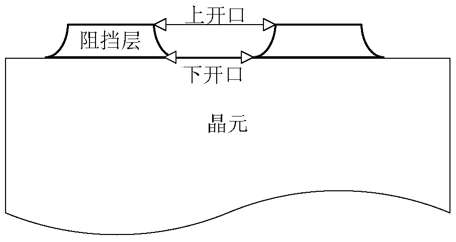
[0050] Step 210: forming a bowl-shaped opening on the front side of the wafer as a barrier layer implanted into the P well;
[0051] Among them, the wafer is the carrier for making Schottky diodes. The front side of the die refers to the side that is used to form the Schottky diode.
[0052] Step 220 : using the bowl-shaped opening as a mask window, injecting ions for forming a P well.
[0053] In the embodiment of the present invention, the self-alignment method of the bowl-shaped opening is used to inject ions for forming the P well. Because the mask window used as the P-well ion implantation is a bowl-shaped opening, the P-well can be fo...
PUM
 Abstract
Description
Claims
Application Information


