Silicon carbide semiconductor device

A silicon carbide and semiconductor technology, applied in the field of silicon carbide semiconductor devices, can solve problems such as narrow current paths and increased on-resistance

Active Publication Date: 2016-05-18
DENSO CORP +1
View PDF6 Cites 15 Cited by
  • Summary
  • Abstract
  • Description
  • Claims
  • Application Information

AI Technical Summary

Problems solved by technology

Therefore, due to the depletion layer extending from the p-type layer, the current path between the p-type layers is narrowed, and the on-resistance increases.

Method used


Image

  • Silicon carbide semiconductor device
  • Silicon carbide semiconductor device
  • Silicon carbide semiconductor device

Examples


no. 1 Embodiment approach

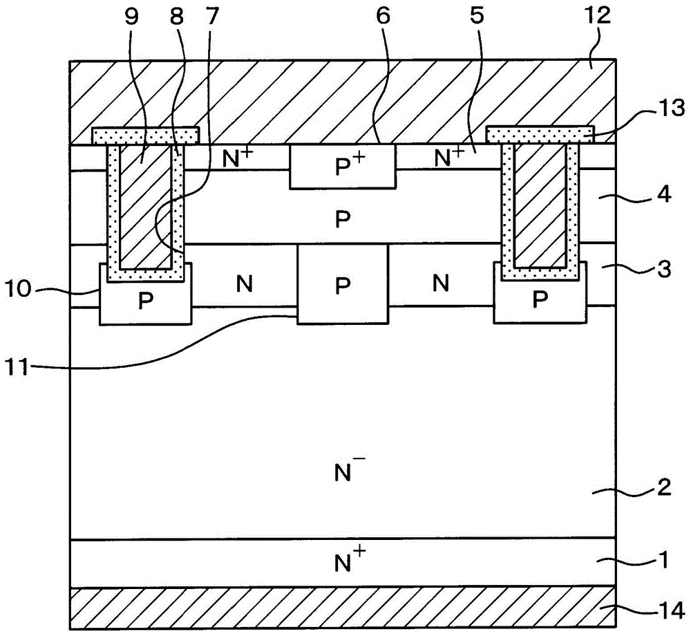
[0028] The first embodiment of the present invention will be described. Here, as an element included in the SiC semiconductor device, a MOSFET with an inverted trench gate structure will be described.

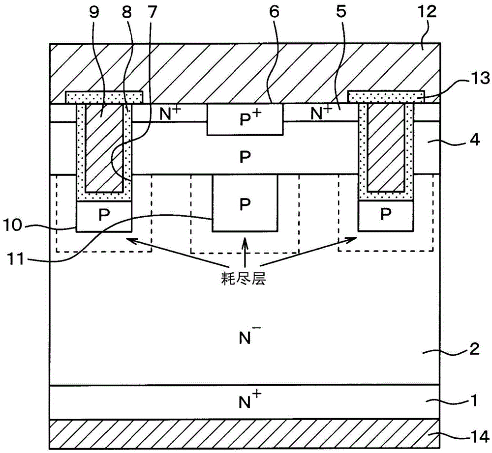
[0029] First, refer to figure 1 The cross-sectional structure of the trench gate structure MOSFET of this embodiment will be described. This figure corresponds to the structure of the MOSFET with 2 cells extracted. Although the figure only shows two-unit MOSFET, it is different from figure 1 In the illustrated MOSFETs, MOSFETs having the same structure are arranged adjacently in multiple columns.

[0030] figure 1 The MOSFET shown uses n + The type layer 1 is formed. n + The type layer 1 is set such that the concentration of n-type impurities such as phosphorus is, for example, 5.0×10 18 ~1.0×10 20 / cm 3 , The thickness is 100~400μm, here the n-type impurity concentration is set to 1.0×10 19 / cm 3 , Set the thickness to 100μm. At that n + On the surface of the type layer 1, n - T...

no. 2 Embodiment approach

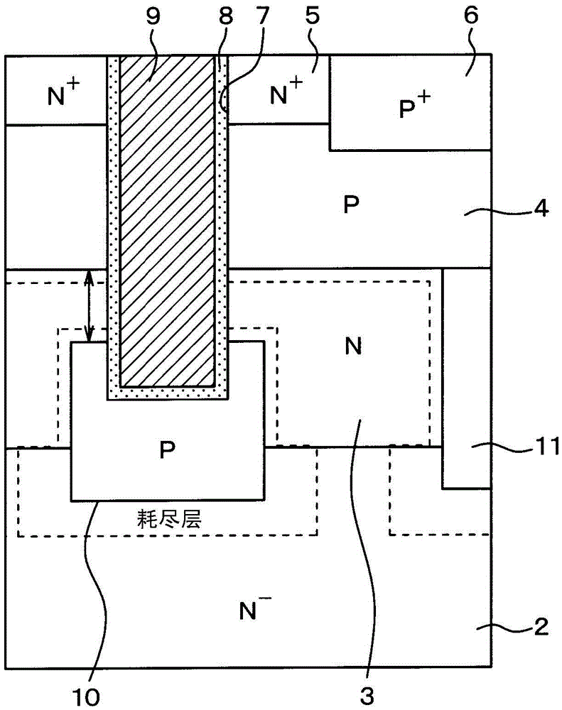
[0085] The second embodiment of the present invention will be described. In this embodiment, the structure of the n-type current diffusion layer 3 is changed from the first embodiment, and the rest is the same as the first embodiment, so only the differences from the first embodiment will be described.

[0086] Such as Picture 9 As shown, in this embodiment, the p-type base region 4 arranged on the n-type current dispersion layer 3 is constituted by a first layer 4a and a second layer 4b having different concentrations. The first layer 4a is the surface side, that is, the p-type base region 4 is located at n + Type 5 and p + The p-type impurity concentration is set to be lower in the portion on the side of the type contact layer 6 than in the second layer 4b. For example, the first layer 4a is set such that the depth to the surface is 0.95 μm, and the p-type impurity concentration is 5.0×10 16 / cm -3 . Since n is formed on the first layer 4a with a depth of 0.5 μm to the surfa...


PUM


Abstract

This silicon carbide semiconductor device has a substrate (1), drift layer (2), current dispersion layer (3), base region (4), source region (5), trench (7), gate insulating film (8), gate electrode (9), source electrode (12), drain electrode (14), and bottom layer (10). The current dispersion layer is formed on the drift layer, and has a first conductivity-type impurity concentration set higher than that of the drift layer. The bottom layer has a second conductivity type, is disposed below the base region, covers a bottom portion of the trench, including corner portions of the bottom portion of the trench, and has more depth than the current dispersion layer.

Description

[0001] Cross-reference of related applications [0002] This application is based on the Japanese application No. 2013-207525 filed on October 2, 2013, and its description is cited here. Technical field [0003] The present application relates to a silicon carbide (hereinafter referred to as SiC) semiconductor device having a trench gate. Background technique [0004] In recent years, SiC has attracted attention as a material for power devices capable of obtaining high electric field breakdown strength. In SiC semiconductor devices, since the electric field breakdown strength is strong, it is possible to control large currents. Therefore, it is expected to be flexibly applied to the control of hybrid motors. [0005] In the SiC semiconductor device, in order to further flow a large current, it is effective to increase the channel density. Therefore, among silicon transistors, trench-gate MOSFETs have been adopted and put into practical use. This trench gate structure is of course ...

Claims


Application Information

Patent Timeline
Patent Type & Authority Applications(China)
IPC IPC(8): H01L29/78H01L29/06H01L29/12
CPCH01L29/7813H01L29/0623H01L29/063H01L29/086H01L29/0878H01L29/1095H01L29/1608H01L29/167H01L29/66068
Inventor 铃木巨裕青井佐智子渡边行彦添野明高小西正树
Owner DENSO CORP
Why Eureka
Try Eureka