Silicon-based plasma ultra wideband terahertz wave absorber

A plasma and ultra-broadband technology, applied in the field of plasma ultra-broadband terahertz wave absorbers, can solve the problems of insufficient bandwidth and low absorption efficiency of terahertz wave absorbers, achieve broad application prospects and application value, reduce The effect of preparation cost and simplified process flow

Inactive Publication Date: 2016-05-25
WUHAN UNIV OF SCI & TECH
View PDF11 Cites 3 Cited by
  • Summary
  • Abstract
  • Description
  • Claims
  • Application Information

AI Technical Summary

Problems solved by technology

[0004] Aiming at the defects and demands of the prior art, the present invention proposes a silicon-based plasma ultra-broadband terahertz wave absorber, the purpose of which is to solve the problems of insufficient bandwidth and low absorption efficiency of existing metamaterial terahertz wave absorbers

Method used


Image

  • Silicon-based plasma ultra wideband terahertz wave absorber
  • Silicon-based plasma ultra wideband terahertz wave absorber
  • Silicon-based plasma ultra wideband terahertz wave absorber

Examples


Embodiment Construction

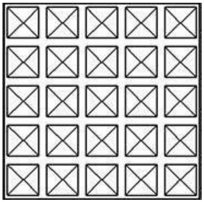
[0026] Such as figure 1 As shown, a silicon-based plasma ultra-broadband terahertz wave absorber proposed by the present invention includes basic units arranged in a moment periodic arrangement, and the basic units are seamlessly connected.

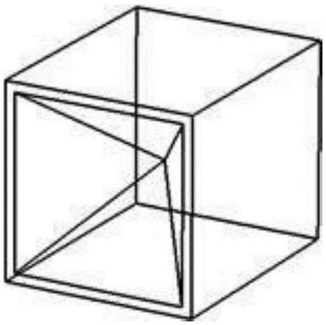
[0027] Such as figure 2 As shown, the basic unit is a rectangular parallelepiped with a square front and a concave quadrangular pyramid on the front. The concave quadrangular pyramid is mainly used to generate the plasmon resonance effect, so that the incident terahertz wave is confined in the structure, and then dissipated by the ohmic loss of the semiconductor material.

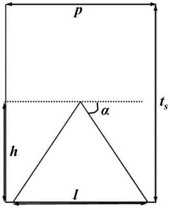
[0028] Such as image 3 As shown, the periodic length p of the basic unit is 50-300 μm, the thickness t s 50-500μm, the notch length l of the quadrangular pyramid is 48-290μm, the notch depth h is 25-250μm, and the inclination angle α≥20°, where l≤p, hs , preferably, the notch depth h of the quadrangular pyramid is the thickness t of the basic unit s The size para...


PUM


Abstract

The invention discloses a silicon-based plasma ultra wideband terahertz wave absorber. The terahertz wave absorber comprises basic units arranged in a periodic array, wherein the front of each basic unit is square and is provided with a hollow rectangular pyramid; the basic units are seamlessly connected; and the material of the terahertz wave absorber is a phosphorus-doped n-type silicon wafer or other semiconductor materials. According to the silicon-based plasma ultra wideband terahertz wave absorber provided by the invention, through a hollow structural design, a wideband plasma resonance effect is generated, so that the absorption rate is strengthened; and meanwhile, the relative bandwidth is greatly improved, the technological process is simplified, and the manufacturing cost is reduced.

Description

technical field [0001] The invention belongs to the technical field of metamaterials and electromagnetic functional materials, and relates to a terahertz wave absorber, in particular to a silicon-based plasma ultra-broadband terahertz wave absorber. Background technique [0002] Terahertz wave absorbers have great application potential in the fields of high-resolution spectral imaging, high data rate short-range communication, material analysis, chemical and biological sensing, and terahertz stealth. At this stage, people have prepared various terahertz wave absorbers by using metamaterial technology, which can realize single-band, multi-band and broadband absorption. The terahertz wave absorber studied at home and abroad is generally an "electric resonator-dielectric layer-metal layer" structure. Its working principle is to independently design the microstructural units that absorb the electric and magnetic responses of electromagnetic waves to generate local electromagneti...

Claims


Application Information

Patent Timeline
Patent Type & Authority Applications(China)
IPC IPC(8): H01Q17/00
CPCH01Q17/00
Inventor 程用志李维刚刘超
Owner WUHAN UNIV OF SCI & TECH
Why Eureka
Try Eureka