Formation method of semiconductor structure

A semiconductor and amorphous silicon technology, applied in semiconductor/solid-state device manufacturing, electrical components, circuits, etc., can solve the problems of fin field effect transistor stability to be improved, and achieve the effect of preventing injection damage

Active Publication Date: 2016-06-01
SEMICON MFG INT (SHANGHAI) CORP
View PDF6 Cites 2 Cited by
  • Summary
  • Abstract
  • Description
  • Claims
  • Application Information

AI Technical Summary

Problems solved by technology

[0004] However, the manufacturing process stability of fin field effect transistors in the prior art still needs to be improved

Method used


Image

  • Formation method of semiconductor structure
  • Formation method of semiconductor structure
  • Formation method of semiconductor structure

Examples


Embodiment Construction

[0032] As mentioned in the background, the manufacturing process stability of the fin field effect transistor in the prior art still needs to be improved. For example, in the manufacturing process of the fin field effect transistor, the problems of fin damage and isolation layer loss will affect The electrical performance of the formed FinFET will be affected.

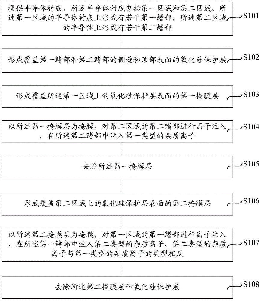
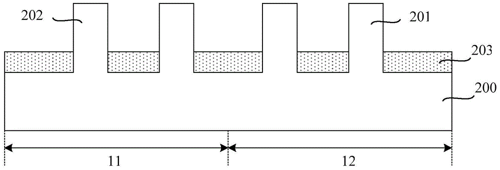
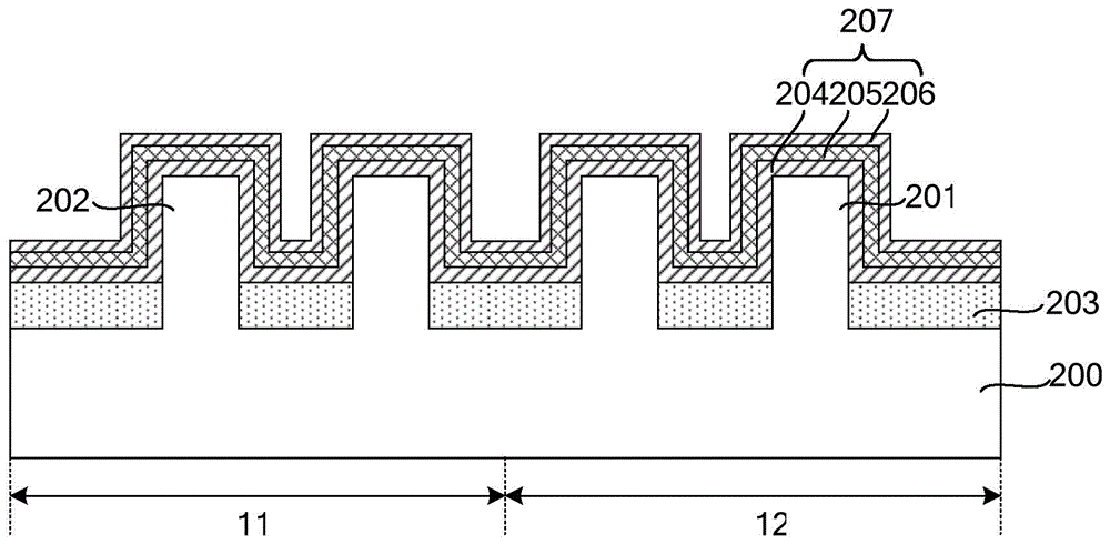
[0033] For the formation process of the fin field effect transistor in the prior art, please refer to figure 1 , comprising, step S101, providing a semiconductor substrate, the semiconductor substrate includes a first region and a second region, a plurality of first fins are formed on the semiconductor substrate in the first region, and a semiconductor substrate in the second region A plurality of second fins are formed on the substrate; step S102, forming a silicon oxide protection layer covering the sidewalls and top surfaces of the first fins and the second fins; step S103, forming an oxide layer covering the first ...


PUM

PropertyMeasurementUnit
thicknessaaaaaaaaaa
thicknessaaaaaaaaaa
thicknessaaaaaaaaaa

Abstract

The present invention provides a formation method of a semiconductor structure. The formation method of the semiconductor structure comprises: providing a semiconductor substrate which has a protruded fin; forming sacrificial layers which are configured to cover the side wall and the top surface of the fin, wherein the sacrificial layers include first silicon oxide layers located at the side wall and the top surface of the fin, an amorphous silicon layers located at the surfaces of the first silicon oxide layers and second silicon oxide layers located at the surface of the amorphous silicon layers; performing ion implantation of the fin, and injecting foreign ions in the fin to form a well region; and removing the sacrificial layers. The formation method of a semiconductor structure is able to prevent a fin from etching and damaging when sacrificial layers are removed while preventing the fin from ion implantation damaging.

Description

technical field [0001] The invention relates to the field of semiconductor manufacturing, in particular to a method for forming a semiconductor structure. Background technique [0002] MOS transistors generate switching signals by regulating the current through the channel region by applying a voltage to the gate. However, when the semiconductor technology enters the node below 20 nanometers, the control ability of the traditional planar MOS transistor on the channel current becomes weak, causing serious leakage current. A Fin Field Effect Transistor (FinFET) is an emerging multi-gate device, which generally includes a semiconductor fin with a high aspect ratio, a gate structure covering part of the top and sidewalls of the fin, and a The source and drain regions in the fins on both sides of the structure, the gate structure of the fin field effect transistor can control the fins from the top and both sides, and has a much stronger gate-to-channel control capability than pl...

Claims


Application Information

Patent Timeline
Patent Type & Authority Applications(China)
IPC IPC(8): H01L21/336
Inventor 毛刚
Owner SEMICON MFG INT (SHANGHAI) CORP
Why Eureka
Try Eureka