A kind of manufacturing method of finfet device

A manufacturing method and device technology, applied in semiconductor/solid-state device manufacturing, semiconductor devices, electrical components, etc., can solve problems such as negative impact on device performance, improve performance and yield, avoid implant damage, and avoid ion implantation shadow effects Effect

Active Publication Date: 2020-06-09
SEMICON MFG INT (SHANGHAI) CORP +1
View PDF4 Cites 0 Cited by
  • Summary
  • Abstract
  • Description
  • Claims
  • Application Information

AI Technical Summary

Problems solved by technology

[0004] At present, it is necessary to implement multi-threshold voltage (multi-Vt) devices on the system-on-chip (SOC) 14nm FinFET, such as figure 1 As shown, a plurality of fins 101 are formed on a semiconductor substrate 100, an isolation structure 102 covering part of the fins 101 is formed on the semiconductor substrate 100, and an exposed surface of the fins 101 and the isolation structure are formed. The oxide layer 103 on the surface of 102 is subjected to threshold voltage ion implantation. The threshold voltage ion implantation is oblique ion implantation, that is, the implantation direction has a certain angle with the surface of the semiconductor substrate. In the traditional process, the threshold voltage is usually passed. Voltage ion implantation is used to modulate the threshold voltage of FINFET devices. Larger dopant implantation angle can increase the sensitivity of ion implantation, but it will cause shadow effects, which will negatively affect the performance of the device.

Method used


Image

  • A kind of manufacturing method of finfet device
  • A kind of manufacturing method of finfet device
  • A kind of manufacturing method of finfet device

Examples


Embodiment 1

[0041] In order to improve the performance of FinFET devices, the present invention proposes a manufacturing method of FinFET devices, such as image 3 As shown, it includes the following main steps:

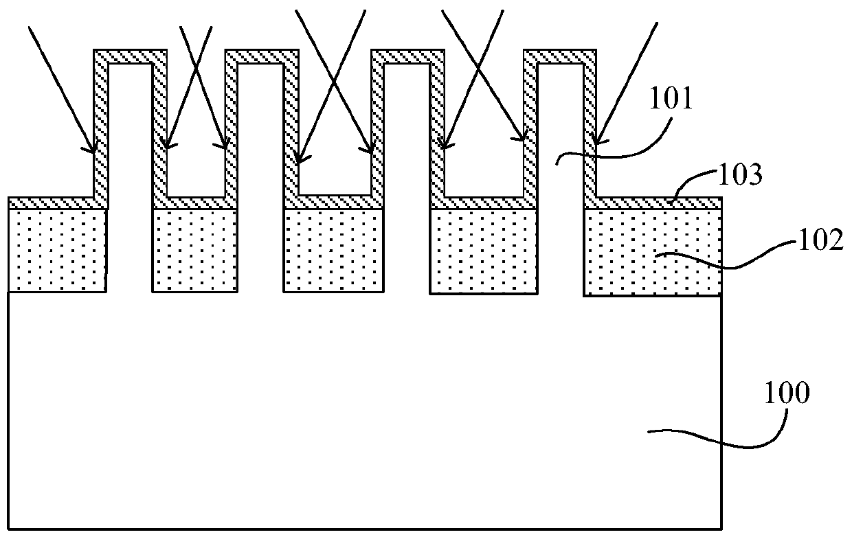
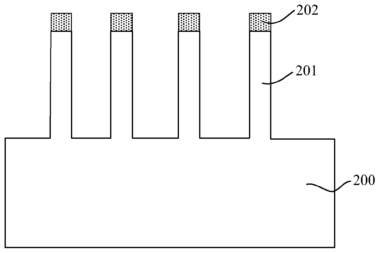
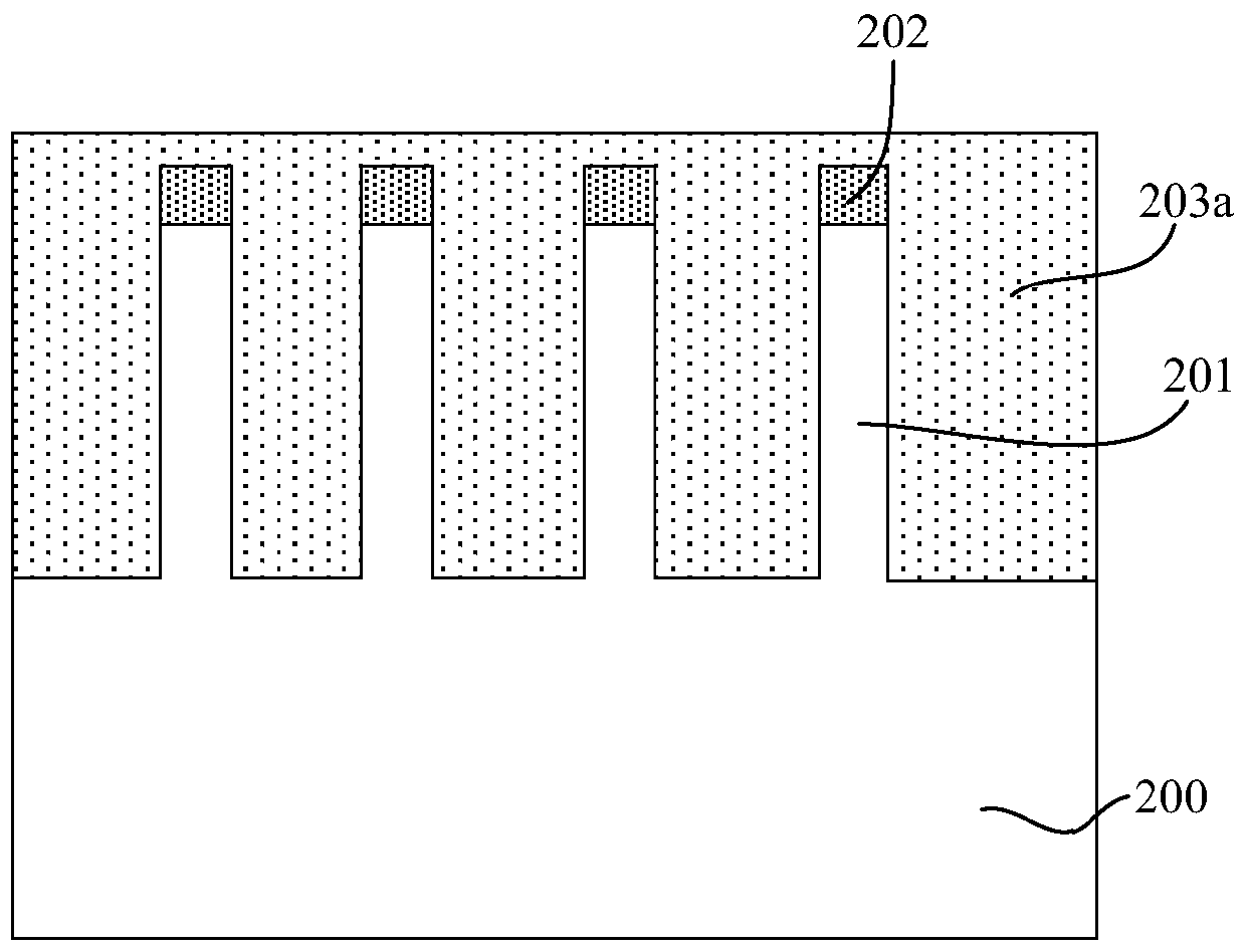
[0042] In step S301, a semiconductor substrate is provided, a plurality of fins are formed on the semiconductor substrate, a hard mask layer is formed on the top of the fins, and the semiconductor substrate between the fins An isolation structure is formed on the bottom, wherein the top surface of the isolation structure is lower than the top surface of the fin;

[0043] In step S302, a first threshold voltage ion implantation is performed to laterally diffuse dopant impurities into the bottom of the fin, and the implantation direction of the first threshold voltage ion implantation is perpendicular to the surface of the semiconductor substrate;

[0044] In step S303, performing a first thermal annealing treatment, so that the dopant impurity implanted into the bottom of the fin ...


PUM


Abstract

The invention provides a FinFET device manufacturing method, and relates to the semiconductor technical field; the method comprises the following steps: providing a semiconductor substrate, forming aplurality of fins on the semiconductor substrate, forming a hard mask layer on the fin top, and forming an isolation structure on the semiconductor substrate between the fins; executing the first threshold-voltage ion implantation, wherein the first threshold-voltage ion implantation direction is vertical to the semiconductor substrate surface; carrying out the first thermal annealing treatment; channeling to stop the ion implantation, and forming a break-through stop layer below a channel zone of the fins; removing the hard mask layer; carrying out the second threshold-voltage ion implantation, and carrying out the second thermal annealing treatment so as to activate doped impurities, thus evenly distributing the doped impurities in the fins. The FinFET device manufacturing method can prevent injection damages on the fins, thus preventing the ion implantation shadow effect caused by inclined injection, and improving the device performance and yield rate.

Description

technical field [0001] The present invention relates to the technical field of semiconductors, in particular to a method for manufacturing a FinFET device. Background technique [0002] With the continuous development of semiconductor technology, in order to improve the performance of the device, the size of integrated circuit devices needs to be continuously reduced. With the continuous reduction of the size of CMOS devices, the development of three-dimensional designs such as fin field effect transistors (FinFET) has been promoted. [0003] Compared with the existing planar transistors, the FinFET device has more superior performance in terms of channel control and reduction of short channel effects (SCE); the planar gate structure is arranged above the channel, while the FinFET The grid is arranged around the fins, so static electricity can be controlled from three sides, and the performance in static electricity control is also more prominent. [0004] At present, it is...

Claims


Application Information

Patent Timeline
Patent Type & Authority Patents(China)
IPC IPC(8): H01L21/336H01L21/265H01L21/266
CPCH01L29/66803
Inventor 周飞
Owner SEMICON MFG INT (SHANGHAI) CORP
Why Eureka
Try Eureka