Semiconductor structures and methods of forming them

A semiconductor and patterning technology, applied in the fields of semiconductor/solid-state device manufacturing, electrical components, circuits, etc., can solve the problems of decreased doping ion concentration, uneven distribution of carriers, leakage of semiconductor devices, etc., to avoid injection damage, Improve the interface quality, improve the effect of isolation effect

Active Publication Date: 2020-07-10
SEMICON MFG INT (SHANGHAI) CORP +1
View PDF4 Cites 0 Cited by
  • Summary
  • Abstract
  • Description
  • Claims
  • Application Information

AI Technical Summary

Problems solved by technology

[0004] The shallow trench isolation structure will exert stress on the active regions on both sides, so that the dopant ion concentration of the channel of the semiconductor device will decrease in the region far from the shallow trench isolation structure, so that the current carrying in the transistor channel region Uneven sub-distribution, leading to problems such as leakage of semiconductor devices, affecting the performance of semiconductor devices

Method used


Image

  • Semiconductor structures and methods of forming them
  • Semiconductor structures and methods of forming them
  • Semiconductor structures and methods of forming them

Examples


Embodiment Construction

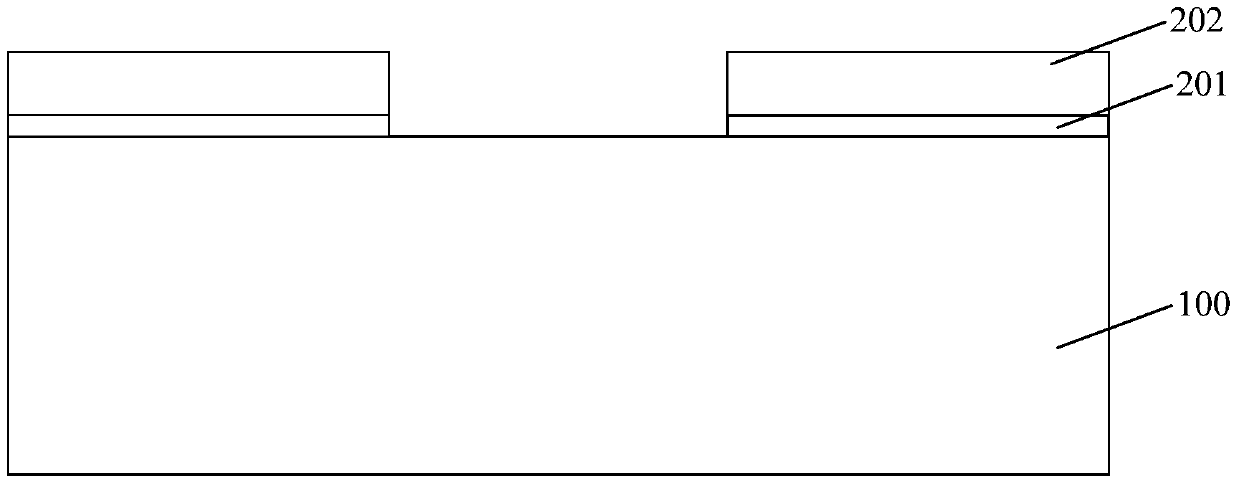
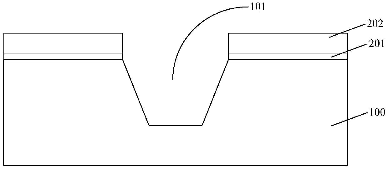
[0029] As mentioned in the background, the shallow trench isolation structure formed in the prior art will lead to uneven carrier concentration distribution in the active regions on both sides, which will affect the performance of semiconductor devices formed on the active regions.

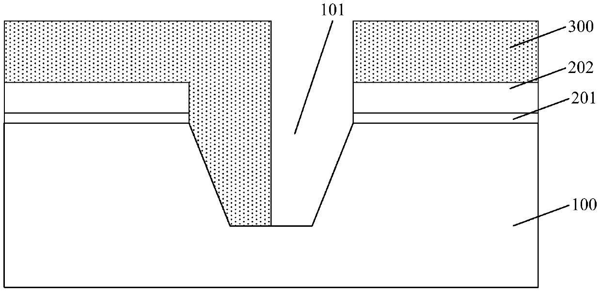
[0030] In an embodiment of the present invention, a doped layer is formed on one side wall of the trench, and the doped layer can prevent the diffusion of dopant ions in the semiconductor substrate, thereby improving the effectiveness of the semiconductor substrate on both sides of the trench. The doping concentration and distribution uniformity of the source region improve the narrow channel effect and negative bias temperature instability (NBTI), thereby improving the performance of semiconductor devices formed on the active region.

[0031] In order to make the above objects, features and advantages of the present invention more comprehensible, specific embodiments of the present invention will ...


PUM

PropertyMeasurementUnit
thicknessaaaaaaaaaa

Abstract

The invention relates to a semiconductor structure and a formation method thereof. The formation method of the semiconductor structure comprises the steps of providing a semiconductor substrate; forming a mask layer with an opening on a surface of the semiconductor substrate; etching the semiconductor substrate along the opening, and forming a groove with a side wall inclining in the semiconductor substrate; forming a doping layer on a surface of the side wall of one side of the groove, wherein the doping layer can be used for preventing doping ions from diffusing in the semiconductor substrate; and filling an isolation layer filled in the groove. By the method, the performance of semiconductor devices formed on active regions at two sides of the isolation layer can be improved.

Description

technical field [0001] The invention relates to the technical field of semiconductors, in particular to a semiconductor structure and a forming method thereof. Background technique [0002] As semiconductor technology enters the deep sub-micron era, components below 0.18 microns (such as between active regions of CMOS integrated circuits) are mostly fabricated using shallow trench isolation (STI) for lateral isolation. An integrated circuit includes many transistors formed on a semiconductor substrate. Generally, the transistors are separated from each other by insulating or isolating structures. A process commonly used to form an isolation structure is a shallow trench isolation (shallow trench isolation, STI for short) process. [0003] The shallow trench isolation process usually forms a trench on a semiconductor substrate, and then fills the trench with an insulating material to form a shallow trench isolation structure. The shallow trench isolation structure surrounds...

Claims


Application Information

Patent Timeline
Patent Type & Authority Patents(China)
IPC IPC(8): H01L21/762
CPCH01L21/76237
Inventor 赵猛
Owner SEMICON MFG INT (SHANGHAI) CORP
Why Eureka
Try Eureka