Dual polycrystal self-aligned complementary bipolar device structure and fabrication method thereof

A technology of bipolar devices and manufacturing methods, applied in semiconductor/solid-state device manufacturing, electric solid-state devices, semiconductor devices, etc., can solve the problems of large investment and high cost, achieve the effect of improving design capabilities and reducing process manufacturing costs

Inactive Publication Date: 2016-06-01
NO 24 RES INST OF CETC
View PDF6 Cites 1 Cited by
  • Summary
  • Abstract
  • Description
  • Claims
  • Application Information

AI Technical Summary

Problems solved by technology

[0004] Aiming at the technical problems of huge investment and high cost in the advanced semiconductor chip processing service factory in the prior art, the present invention provides a double-poly self-aligning chip that can realize the next-level higher technology node designed for the capacity of the o

Method used


Image

  • Dual polycrystal self-aligned complementary bipolar device structure and fabrication method thereof
  • Dual polycrystal self-aligned complementary bipolar device structure and fabrication method thereof
  • Dual polycrystal self-aligned complementary bipolar device structure and fabrication method thereof

Examples


Embodiment Construction

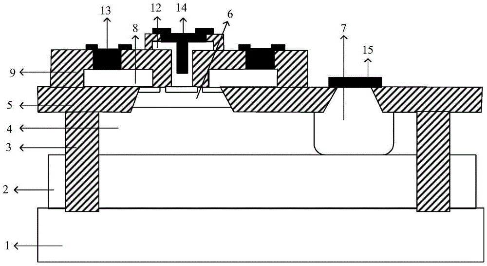
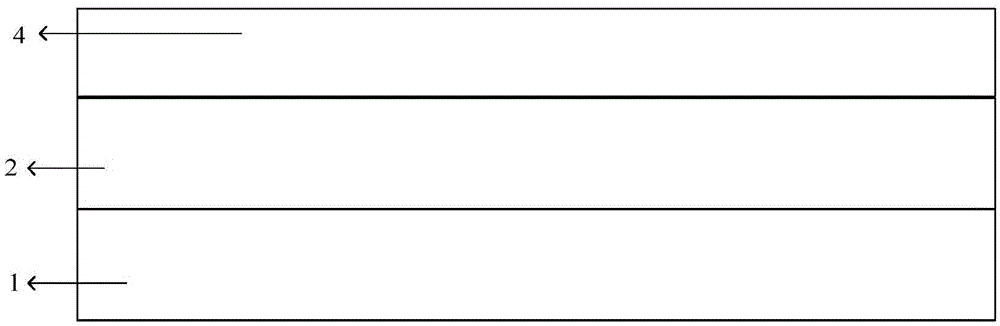
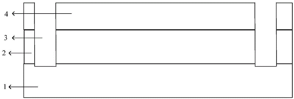
[0049] In order to make the technical means, creative features, goals and effects achieved by the present invention easy to understand, the present invention will be further described below in conjunction with specific illustrations.

[0050] In describing the present invention, it is to be understood that the terms "width", "depth", "upper", "lower", "front", "rear", "left", "right", "vertical", " The orientation or positional relationship indicated by "horizontal" and so on is based on the orientation or positional relationship shown in the drawings, which is only for the convenience of describing the present invention and simplifying the description, rather than indicating or implying that the referred device or element must have a specific orientation, so as to Specific orientation configurations and operations, therefore, are not to be construed as limitations on the invention.

[0051] In order to achieve the purpose of the present invention, the present invention elabor...


PUM


Abstract

The invention provides a dual polycrystal self-aligned complementary bipolar device structure and a fabrication method thereof. Process development of a 0.35micron technology node is achieved under the condition of a 6inch process line, namely on the process line of photoetching the technology node with the minimum linewidth of 0.5micron; fabrication of a complementary bipolar process device which can only be achieved under a higher technology level is achieved under the premise of not increasing equipment budget of the higher technology level of the 6inch process line; the actual minimum process dimension reaches 0.3-0.35micron; the device performance is not reduced, namely various technical indexes of a device all reach the technology level under the 0.35micron technology node and the characteristic frequency of the device employing an NPN tube and a PNP tube reaches the magnitude of gigahertz; and on the basis of high structure symmetry of the longitudinal NPN tube and PNP tube and high symmetry of device characteristics, a technology platform and an important guarantee are provided for improving the design capability of a push-pull circuit. Due to the adoption of the 6inch process line, the actual process fabrication cost is effectively reduced.

Description

technical field [0001] The invention belongs to the field of complementary bipolar transistor devices, and in particular relates to a double-polycrystalline self-aligned complementary bipolar device structure and a manufacturing method thereof. Background technique [0002] like figure 1 Shown is a schematic cross-sectional structure diagram of an existing conventional double polycrystalline self-aligned complementary bipolar transistor, which mainly includes a single crystal silicon substrate, a deep trench dielectric isolation structure, a buried layer structure, an epitaxial structure, and a local oxide layer (LOCOS) structure, Extrinsic base structure, intrinsic base structure and emitter structure, etc. [0003] Bipolar transistors have important applications in analog and mixed-signal integrated circuits (ICs) due to their excellent current drive capability, linearity and good matching. The dual polycrystalline self-aligned complementary bipolar process is an advance...

Claims


Application Information

Patent Timeline
IPC IPC(8): H01L21/8228H01L27/102
CPCH01L21/8228H01L27/1022
Inventor 张培健唐昭焕胡刚毅易前宁杨永晖刘勇钟怡陈文锁谭开洲朱坤峰
Owner NO 24 RES INST OF CETC
Why Eureka
Try Eureka