Tunneling field effect transistor and manufacturing method thereof

A technology of tunneling field effect and manufacturing method, applied in semiconductor/solid-state device manufacturing, semiconductor devices, electrical components, etc., can solve problems such as disadvantages, small TFET tunneling current, MOSFET self-alignment process is no longer applicable, etc. The effect of small device size and improved integration

Inactive Publication Date: 2016-06-01
INST OF MICROELECTRONICS CHINESE ACAD OF SCI
View PDF7 Cites 5 Cited by
  • Summary
  • Abstract
  • Description
  • Claims
  • Application Information

AI Technical Summary

Problems solved by technology

[0004] However, limited by the tunneling probability, the tunneling current of the traditional TFET is small. At the same time, because the doping type of the source and drain of th...

Method used


Image

  • Tunneling field effect transistor and manufacturing method thereof
  • Tunneling field effect transistor and manufacturing method thereof
  • Tunneling field effect transistor and manufacturing method thereof

Examples


Embodiment Construction

[0037] Embodiments of the present invention are described in detail below, examples of which are shown in the drawings, wherein the same or similar reference numerals designate the same or similar elements or elements having the same or similar functions throughout. The embodiments described below by referring to the figures are exemplary only for explaining the present invention and should not be construed as limiting the present invention.

[0038] The invention aims at proposing a new tunneling field effect transistor structure to meet the requirement of continuously reducing device size. refer to Figure 8 As shown, the tunneling field effect transistor includes:

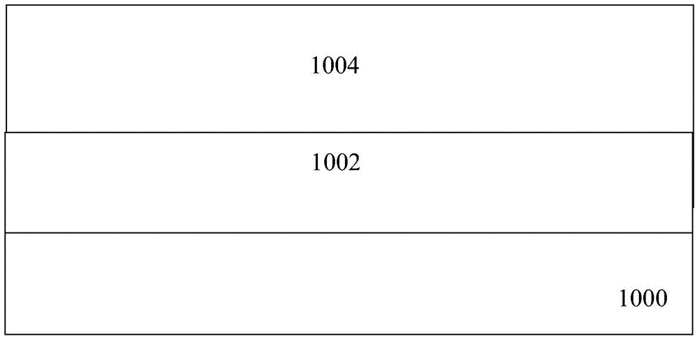
[0039] substrate 1000;

[0040] a drain region 2002 having a first doping type on the substrate;

[0041] a channel region 2004 above the drain region;

[0042] a source region 2006 having a second doping type above the channel region;

[0043] A drain connection region 2003 above the substrate and connecte...


PUM


Abstract

The present invention provides a tunneling field effect transistor. The tunneling field effect transistor comprises: a substrate; a drain region with a first doped type disposed on the substrate; a channel region arranged above the drain region; a source region with a second doped type arranged above the channel region; a drain region connection region, arranged on the substrate, connected with the side wall of the drain region; a gate dielectric layer arranged at the side walls of the source region, the drain region and channel region; a gate electrode arranged at the side wall of the gate dielectric layer; and an insulation layer between the gate electrode and the drain region connection region. According to the invention, a source region and a drain region are formed in the vertical direction of the substrate, and a tunneling field effect transistor with a vertical structure is formed; and moreover, the tunneling field effect transistor has smaller size of a device to satisfy the requirement of continuously decreased size of the device, so that the integration level is improved.

Description

technical field [0001] The invention relates to the field of semiconductor devices, in particular to a tunneling field effect transistor and a manufacturing method thereof. Background technique [0002] With the continuous shrinking of device size, the number of devices on a chip per unit area is increasing, which will lead to an increase in dynamic power consumption. At the same time, the continuous shrinking of device size will inevitably lead to an increase in leakage current, which in turn will cause an increase in static power consumption. . For traditional Metal Oxide Field Effect Transistor (MOSFET) devices, limited by carrier Boltzmann thermal distribution, the subthreshold swing (SS) of MOSFET devices must be greater than 60mV / decade, which seriously affects the The switching rate at the lower voltage causes the leakage current to increase exponentially with the decrease of the supply voltage, and thus the static power consumption increases exponentially. [0003]...

Claims


Application Information

Patent Timeline
IPC IPC(8): H01L29/78H01L21/336
Inventor 许高博徐秋霞
Owner INST OF MICROELECTRONICS CHINESE ACAD OF SCI
Why Eureka
Try Eureka