Mott transistor and fabrication method thereof

A transistor and Mott technology, applied in the field of Mott transistors and preparation, can solve the problems of thermal stability of leakage and poor stability of Mott transistors, and achieve the effect of solving leakage and poor thermal stability and ensuring stability.

Inactive Publication Date: 2016-06-01
NINGBO INST OF MATERIALS TECH & ENG CHINESE ACADEMY OF SCI
View PDF5 Cites 9 Cited by
  • Summary
  • Abstract
  • Description
  • Claims
  • Application Information

AI Technical Summary

Problems solved by technology

[0003] Based on this, it is necessary to provide a Mott transistor and its preparation method for the traditional use of ionic liquid as the gate

Method used


Image

  • Mott transistor and fabrication method thereof
  • Mott transistor and fabrication method thereof
  • Mott transistor and fabrication method thereof

Examples


preparation example Construction

[0046] Specifically, the structure of the Mott transistor of the present invention can be either a top-gate structure or a bottom-gate structure. Therefore, the Mott transistor preparation method provided by the present invention specifically includes the following steps:

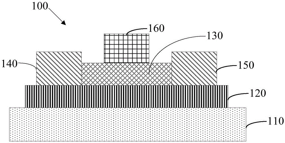
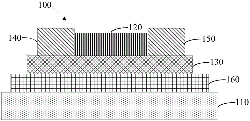
[0047] First, through step S100, the gate electrode 160 is prepared on the surface of the substrate 110 by a coating process, and then the gate dielectric layer 130 and the channel layer 120 are sequentially prepared on the surface of the gate electrode 160, and then through step S200, A source electrode 140 and a drain electrode 150 are prepared on the surface of the gate dielectric layer 130 covered by the gate dielectric layer 120 . In this way, the preparation of the bottom-gate Mott transistor 100 can be completed.

[0048] Or, first, through step S100', the channel layer 120 and the gate dielectric layer 130 are sequentially prepared on the surface of the substrate 110 by using a coating process, and...

Embodiment 1

[0054] This example provides figure 1 A fabrication method of an all-solid-state metal-insulator transition Mott (Mott) transistor 100 with a top-gate structure is shown. Wherein, the substrate 110 is thermal silicon oxide, and the gate dielectric layer 130 is silicon dioxide (SiO 2 ) film, the channel layer 120 is vanadium dioxide (VO 2 ) film, the gate 160, the source 140 and the drain 150 are Ti / Au composite films.

[0055] The manufacturing method of the all-solid-state metal-insulator transition Mott (Mott) transistor 100 of the top gate structure of the present embodiment includes the following steps:

[0056] Step 1: Clean thermal silica by ultrasonic cleaning with acetone, absolute ethanol and deionized water.

[0057] Step 2: Deposit a layer of vanadium dioxide (VO 2 ) film as the channel layer 120. Wherein, the process condition when adopting the magnetron sputtering technology to deposit the channel layer 120 is: the vacuum degree of the vacuum chamber of the m...

Embodiment 2

[0063] This embodiment also provides figure 1 A fabrication method of an all-solid-state metal-insulator transition Mott (Mott) transistor 100 with a top-gate structure is shown. Wherein, in this embodiment, the substrate 110 in the Mott transistor 100 is sapphire, and the gate dielectric layer 130 is aluminum oxide (Al 2 o 3 ) film, the channel layer 120 is a cobalt oxide (CoO) film, and the gate 160, source 140 and drain 150 are Ti / Au composite films.

[0064] The manufacturing method of the all-solid-state metal-insulator transition Mott (Mott) transistor 100 of the top gate structure of the present embodiment includes the following steps:

[0065] Step 1: Ultrasonic cleaning of clean sapphire with acetone, absolute ethanol and deionized water.

[0066] Step 2: Deposit a cobalt oxide (CoO) thin film on the sapphire as the channel layer 120 by magnetron sputtering technology.

[0067] Step 3: Deposit a Ti / Au composite film on the cobalt oxide (CoO) film as the source ele...


PUM

PropertyMeasurementUnit
Power densityaaaaaaaaaa
Thicknessaaaaaaaaaa
Thicknessaaaaaaaaaa

Abstract

The invention discloses a Motto transistor and a fabrication method thereof. The method comprises the following steps of fabricating a grid on the surface of a substrate by a coating technique, and sequentially fabricating a grid dielectric layer and a channel layer on the surface of the grid; and fabricating a source and a drain on the surface, which is not covered by the channel layer, of the grid dielectric layer, and completing the fabrication of the Mott transistor with a bottom gird structure; or sequentially fabricating the channel layer and the grid dielectric layer on the surface of the substrate by the coating technique, fabricating the source and the drain on the surface, which is not covered by the grid dielectric layer, of the channel layer, fabricating the grid on the surface of the grid dielectric layer, and completing the fabrication of the Mott transistor with a top grid structure, wherein the channel layer is a Mott insulation body thin film, and the grid dielectric layer is a solid-state oxide proton conductor film. By the method, the full-solid-state structure of the Mott transistor is achieved, thus, the problems of liquid leakage and poor thermal stability are prevented when the fabricated Mott transistor is in Mott conversion, and finally, the problem of relatively poor stability of a traditional Mott transistor is effectively solved.

Description

technical field [0001] The invention relates to the technical field of semiconductor devices, in particular to a Mott transistor and a preparation method. Background technique [0002] Mott insulator is an insulator with strong electron correlation effect, which can cause metal-insulator Mott transition of Mott insulator through heat, light and electric field, which makes Mott insulator can be applied to window coating, new Solid-state memory, metamaterials, Mott field-effect transistors and other fields. At present, Mott transistors prepared using Mott insulators usually use vanadium dioxide (VO 2 ) as the channel layer of the transistor, and the ionic liquid as the gate dielectric layer of the transistor, the metal-insulator Mott transformation of vanadium dioxide occurs at a relatively high temperature through electrostatic regulation. However, when ionic liquid is used as the gate dielectric layer of the Mott transistor, the stability of the Mott transistor is poor due...

Claims


Application Information

Patent Timeline
IPC IPC(8): H01L49/00
CPCH10N99/03
Inventor 张洪亮曹鸿涛李龙张莉莉
Owner NINGBO INST OF MATERIALS TECH & ENG CHINESE ACADEMY OF SCI
Why Eureka
Try Eureka