Signal conversion device and method

A signal conversion device and signal technology, applied in the direction of standard conversion, film film standard conversion, image communication, etc.

Active Publication Date: 2016-06-01
KUSN INFOVISION OPTOELECTRONICS
View PDF4 Cites 11 Cited by
  • Summary
  • Abstract
  • Description
  • Claims
  • Application Information

AI Technical Summary

Problems solved by technology

When testing the above-mentioned display module, the test device needs to output the test signal corresponding to the display module. For example, the test device of the display module of the MIPI interface needs to output the MIPI test signal, and the test device of the display module of the eDP interface needs Output eDP test signal. The test device of the display module with TTL interface needs to output TTL test signal. However, the existing test device does not have this function, because most of the test devices are LVDS interface, which can only output multi-channel LVDS signal, and ordinary display modules continue to be produced, and their test devices have not entered the replacement cycle and will continue to be used
Although display module manufacturers also produce display modules with MIPI, TTL, eDP and other interfaces, in order to protect investment and reduce production costs, it is impossible to eliminate the existing test equipment and re-purchase expensive MIPI, TTL, eDP interface displays in large quantities. Module dedicated test device

Method used


Image

  • Signal conversion device and method
  • Signal conversion device and method
  • Signal conversion device and method

Examples


no. 1 example

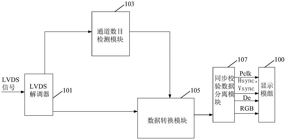
[0021] figure 1 is a structural block diagram of the signal conversion device provided by the first embodiment of the present invention. The signal conversion device is used to convert the LVDS signal output by the LVDS interface into a TTL signal and provide it to the display module. Please refer to figure 1 , the signal conversion device includes an LVDS demodulator 101, a channel number detection module 103, a data conversion module 105, and a synchronization verification data separation module 107. Wherein, the signal conversion device may be integrated into an FPGA (Field-Programmable Gate Array, ie Field-Programmable Gate Array) chip.

[0022] Specifically, the LVDS demodulator 101 is connected to the channel number detection module 103 and the data conversion module 105, and is used to receive and demodulate the LVDS signals output by multiple channels of the LVDS interface, and convert the demodulated LVDS signals of multiple channels The signal is provided to the c...

no. 2 example

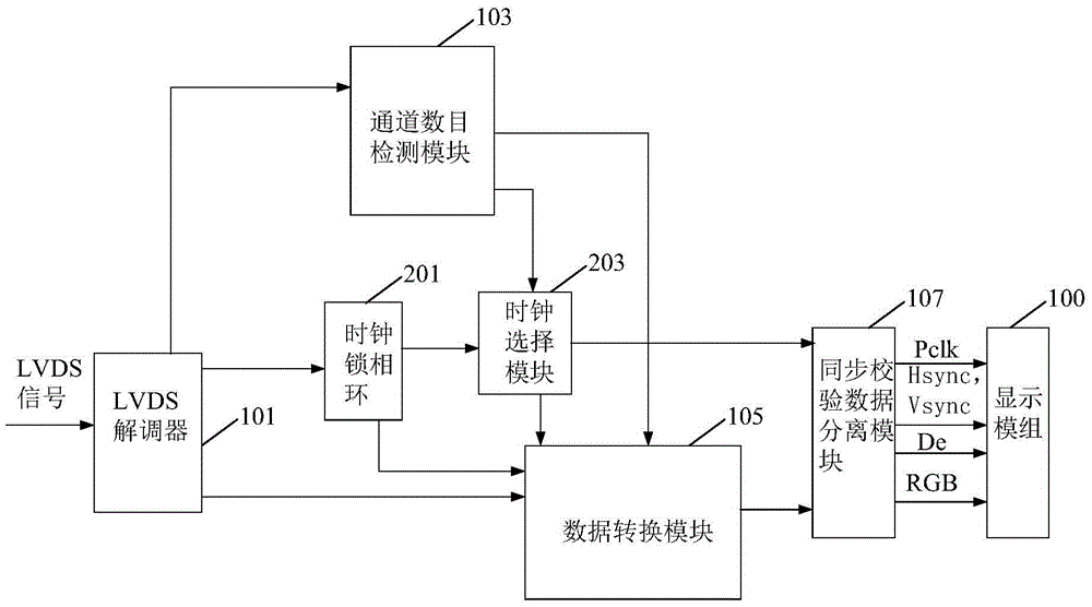
[0034] figure 2 is a structural block diagram of the signal conversion device provided by the second embodiment of the present invention. figure 2 is in figure 1 improved on the basis of figure 2 and figure 1 The difference is that figure 2 The signal conversion device may further include: a clock phase-locked loop 201 and a clock selection module 203 .

[0035] The clock phase-locked loop 201 is connected with the LVDS demodulator 101, the clock selection module 203, and the data conversion module 105, and is used for latching and multiplying the pixel clock signal in the LVDS signal of the demodulated first channel to generate Multiple pixel clock signals are generated, and the generated multiple pixel clock signals are provided to the clock selection module 203 and the data conversion module 105 . For example, the clock phase-locked loop 201 can generate a single-channel pixel clock signal, such as a double-frequency pixel clock signal, or a dual-channel pixel cloc...

no. 3 example

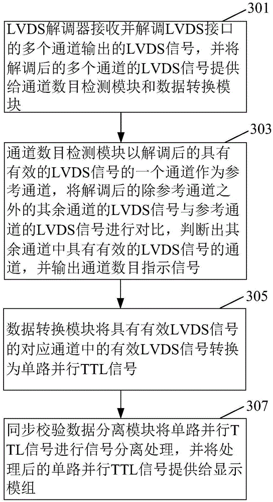
[0041] image 3 It is a flow chart of the steps of the signal conversion method provided by the third embodiment of the present invention. The method is applied to the above-mentioned signal conversion device, please refer to image 3 , the signal conversion method of this embodiment includes the following steps 301-307.

[0042] In step 301, the LVDS demodulator receives and demodulates LVDS signals output by multiple channels of the LVDS interface, and provides the demodulated LVDS signals of multiple channels to the channel number detection module and the data conversion module, and the multiple channels include the first One to the nth channel, where n is an integer greater than 0;

[0043] Step 303, the channel number detection module uses a channel with an effective LVDS signal after demodulation as a reference channel, compares the LVDS signals of other channels except the reference channel after demodulation with the LVDS signal of the reference channel, and judges ...


PUM


Abstract

Embodiments of the invention disclose a signal conversion device and method. The signal conversion device comprises an LVDS (Low Voltage Differential Signaling) demodulator, a channel number detection module, a data conversion module and a synchronous check data separation module, wherein the LVDS demodulator is used for receiving and demodulating LVDS signals output by a plurality of channels of an LVDS interface; the channel number detection module is used for taking one channel provided with an effective LVDS signal after demodulation as the reference channel, carrying out comparison on the LVDS signals of the remaining channels except for a reference channel after demodulation and the LVDS signal of the reference channel, judging the channels provided with the effective LVDS signals in the remaining channels, and outputting a channel number indication signal; the data conversion module is used for converting the effective LVDS signals in the corresponding channels provided with effective LVDS signals into one way of parallel TTL (Transistor-Transistor Logic) signals; and the synchronous check data separation module is used for carrying out signal separation processing on one way of parallel TTL signals. According to the signal conversion device and method, the number of the LVDS channels can be automatically recognized, and the device and the method have the advantages of simplicity in operation, high efficiency and low cost.

Description

technical field [0001] The invention relates to the field of display technology, in particular to a signal conversion device and method. Background technique [0002] At present, in order to meet people's continuous pursuit of higher definition and more realistic display effects on various consumer electronic devices (such as mobile devices, etc.), display modules are moving towards ultra-high resolution and ultra-high pixel density. Development, usually the interface of this display module mostly adopts TTL (TransistorTransistorLogic, transistor-transistor logic), MIPI (MobileIndustryProcessorInterface, mobile industry processor interface), eDpeDP and other interfaces. When testing the above-mentioned display module, the test device needs to output the test signal corresponding to the display module. For example, the test device of the display module of the MIPI interface needs to output the MIPI test signal, and the test device of the display module of the eDP interface ne...

Claims


Application Information

Patent Timeline
Patent Type & Authority Applications(China)
IPC IPC(8): H04N7/01H04N5/765G09G3/00
CPCH04N5/765H04N7/0115G09G3/006
Inventor 雷雪梅
Owner KUSN INFOVISION OPTOELECTRONICS
Why Eureka
Try Eureka