Production method of self-alignment MOSFET device

A technology of MOS devices and manufacturing methods, applied in semiconductor/solid-state device manufacturing, semiconductor devices, electrical components, etc., to achieve the effects of improving radio frequency characteristics, reducing parasitic capacitance, and improving consistency

Inactive Publication Date: 2016-06-08
DONGGUAN QINGMAITIAN DIGITAL TECH
View PDF3 Cites 3 Cited by
  • Summary
  • Abstract
  • Description
  • Claims
  • Application Information

AI Technical Summary

Problems solved by technology

However, there are many different physical and chemical properties from III-V semiconductor devices and silicon

Method used


Image

  • Production method of self-alignment MOSFET device
  • Production method of self-alignment MOSFET device
  • Production method of self-alignment MOSFET device

Examples


Embodiment Construction

[0034] In order to make the object, technical solution and advantages of the present invention clearer, the present invention will be described in further detail below in conjunction with specific embodiments and with reference to the accompanying drawings.

[0035] Such as figure 1 As shown in -9, the schematic diagram of the production process of the source-drain self-aligned MOS device provided by the present invention, the present invention provides a source-drain self-aligned MOS device and a production method thereof, and its production process is as follows:

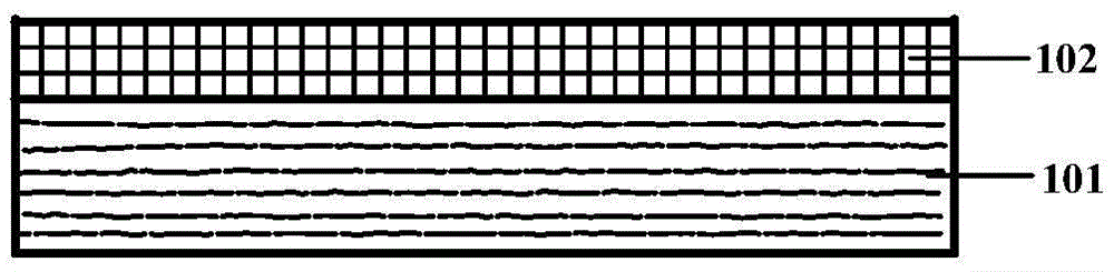
[0036] (1) an indium phosphide single crystal substrate layer;

[0037] (2) if figure 1 As shown, the InGaAs channel layer (102) formed on the single crystal substrate;

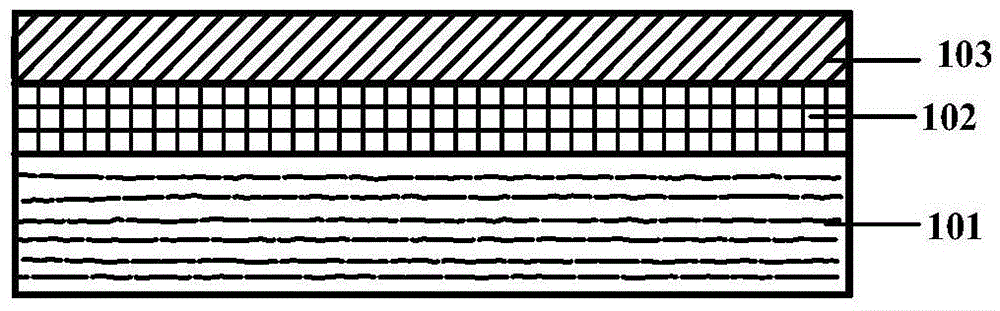
[0038] (3) if figure 2 As shown, an InP / InGaAs composite source-drain ohmic contact layer (103) is formed on the InGaAs channel layer (102);

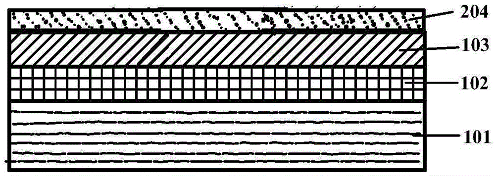
[0039] (4) if image 3 As shown, a low-K dielectric silicon dioxide (204) is deposited on the ohm...


PUM

PropertyMeasurementUnit
Thicknessaaaaaaaaaa

Abstract

The invention discloses an III-V MOS device and a production method. The production method comprises the following sequential steps: forming a channel layer on a semiconductor layer on a substrate; forming an ohmic contact layer on the semiconductor channel layer; making silicon dioxide medium pores in the ohmic contact layer; etching the ohmic contact layer by an etching method; making a SiO2 side wall; depositing a high-k medium in the channel by an atom layer depositing method; making a gate metal; etching the high-k medium and silicon dioxide except the gate metal by taking the gate metal as a mask to expose the ohmic contact layer; and depositing source-drain metals in an active area by an evaporation technology to finish the production of the MOSFET device. The production method of the device can be used for producing a digital integrated circuit; and after the production of gate and source and gate-source gap, the radio-frequency characteristic is improved, and the method also can be applied to a radio-frequency integrated circuit.

Description

technical field [0001] The invention relates to the technical field of semiconductor integrated circuit manufacturing, in particular to a method for epitaxially growing a III-V channel layer on a single crystal substrate and making a self-aligned source-drain MOS device, which is applied to high-performance CMOS technology field. Background technique [0002] Compared with silicon materials, Ⅲ-Ⅴ compound semiconductor materials have the advantages of high carrier mobility and large forbidden band width, and have good characteristics in thermal, optical and electromagnetic aspects. After silicon-based CMOS technology is approaching its physical limit, III-V compound semiconductor materials may become candidate channel materials due to their high electron mobility characteristics for making CMOS devices. However, there are many different physical and chemical properties between III-V semiconductor devices and silicon devices, and the MOS structure and process suitable for sil...

Claims


Application Information

Patent Timeline
IPC IPC(8): H01L21/336H01L21/28
CPCH01L29/4236H01L29/454H01L29/66522H01L29/66575
Inventor 刘丽蓉
Owner DONGGUAN QINGMAITIAN DIGITAL TECH
Why Eureka
Try Eureka