
Organic electroluminescent displayer and manufacturing method thereof

A manufacturing method and technology of an organic light-emitting layer, applied in the manufacture of semiconductor/solid-state devices, electric solid-state devices, circuits, etc., can solve the problems of reducing the luminous efficiency of OLED displays, and achieve the goals of improving luminous efficiency, preventing color mixing, and reducing total reflection Effect

Inactive Publication Date: 2016-06-08
王金
View PDF0 Cites 1 Cited by
  • Summary
  • Abstract
  • Description
  • Claims
  • Application Information

AI Technical Summary

Problems solved by technology

However, the filler can absorb part of the light emitted by the OLED, reducing the luminous efficiency of the OLED display

Method used


Image

  • Organic electroluminescent displayer and manufacturing method thereof
  • Organic electroluminescent displayer and manufacturing method thereof
  • Organic electroluminescent displayer and manufacturing method thereof

Examples


Embodiment 1

[0043] Embodiment 1 of the present invention provides an organic electroluminescent display, hereinafter referred to as an OLED display.

[0044] An OLED display may include a driving unit and a panel. The driving unit may include a timing controller, a scan driver and a data driver. A panel may include pixels. The pixels may be arranged in a basic matrix pattern. The pixels can be controlled in different ways and can emit light in different ways to display images across the entire surface of the panel. A pixel may include an organic light emitting layer and a thin film transistor. The organic light emitting layer may emit light by itself. The thin film transistor can drive the organic light emitting layer and control the brightness of the organic light emitting layer. The thin film transistor can control the pixel to receive or not receive the data signal in response to the scan-on voltage of the scan signal, thereby controlling the brightness of the organic light emitti...

Embodiment 2

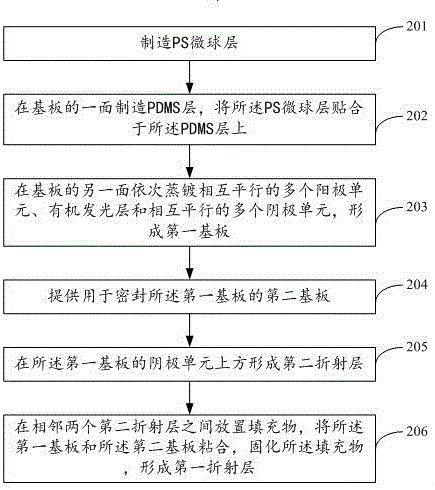
[0071] Embodiment 2 of the present invention provides a method for manufacturing an organic electroluminescent display according to Embodiment 1, such as figure 2 As shown, the method includes:

[0072] 201. Manufacturing PS microsphere layer 11;

[0073] Wherein, the PS microsphere layer 11 is a single-layer structure composed of PS microspheres. This step specifically includes:

[0074] 2011. Dissolving the PS microsphere raw material into ethanol to form a mixed solution, and dropping the mixed solution into water to form a suspension;

[0075] 2012. Clean the carrier sheet, soak the carrier sheet in hydrogen peroxide solution for 3 minutes, dry, dry or treat with plasma;

[0076] 2013. Put the carrier sheet into the petri dish, add water to the petri dish, drop the suspension of PS microspheres on the surface of the water to form a single layer of PS microspheres;

[0077] In 2014, using the vertical deposition method, the carrier sheet was slowly pulled out of the so...


PUM


Abstract

The invention discloses an organic electroluminescent displayer and a manufacturing method thereof and belongs to the technical field of displayer manufacturing. The organic electroluminescent displayer comprises a PS microsphere layer embedded in one side of a PDMS layer; a substrate, a plurality of parallel positive electrode units, an organic light emitting layer and a plurality of parallel negative electrode units are sequentially arranged on the other side of the PDMS layer; the positive electrode units and the negative electrode units are parallel and staggered; the organic light emitting layer is provided with a first refraction layer, the negative electrode units are provided with second refraction layers, and the refractive index of the first refraction layer is larger than that of the second first refraction layers. By means of the organic electroluminescent displayer and the manufacturing method thereof, light emitting efficiency of the organic electroluminescent displayer can be improved, double-side light emission is achieved, and color mixing between pixels is prevented.

Description

technical field [0001] The invention relates to the technical field of display devices, in particular to an organic electroluminescence display and a manufacturing method thereof. Background technique [0002] Organic Light-Emitting Diodes (OLED for short) is a self-luminous display, which is light in weight, ultra-thin, high in theoretical luminous efficiency, and more importantly, it can be made flexible. Whether it is in the field of lighting or display, it will is the future direction of development. [0003] An OLED display generally includes a thin film transistor and an OLED for each of a plurality of pixels formed on a substrate, and is sealed with, for example, a sealing member such as a glass material. Seals prevent moisture and impurities from penetrating into each OLED and TFT. In addition, fillers are often interposed between the seal and the substrate. The filler can protect the OLED by absorbing external impact, and can cool the OLED by absorbing heat emitt...

Claims


Application Information

Patent Timeline
Patent Type & Authority Applications(China)
IPC IPC(8): H01L27/32H01L51/52H01L51/56
CPCH10K59/12H10K50/858H10K71/00
Inventor 冯团辉王利敏张元敏王红玲殷志锋王金
Owner 王金
Learn More