Low temperature polysilicon thin film transistor and its manufacturing method

A technology of thin-film transistors and low-temperature polysilicon, which is applied in the direction of transistors, semiconductor/solid-state device manufacturing, semiconductor devices, etc., can solve the problems of abnormal electrical properties of TFT devices, unsatisfactory activation and hydrogenation effects, etc., so as to improve utilization rate and hydrogenation effect, the effect of increasing the activation effect

Active Publication Date: 2019-07-26
WUHAN CHINA STAR OPTOELECTRONICS TECH CO LTD
View PDF5 Cites 0 Cited by
  • Summary
  • Abstract
  • Description
  • Claims
  • Application Information

AI Technical Summary

Problems solved by technology

However, because the dielectric layer is far away from the polysilicon, the effect of activation and hydrogenation is not ideal, which easily causes problems such as abnormal electrical properties of TFT devices.

Method used


Image

  • Low temperature polysilicon thin film transistor and its manufacturing method
  • Low temperature polysilicon thin film transistor and its manufacturing method
  • Low temperature polysilicon thin film transistor and its manufacturing method

Examples


Embodiment Construction

[0030] This embodiment provides a low-temperature polysilicon thin film transistor, and its fabrication method is as follows:

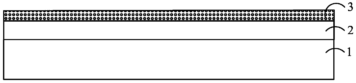
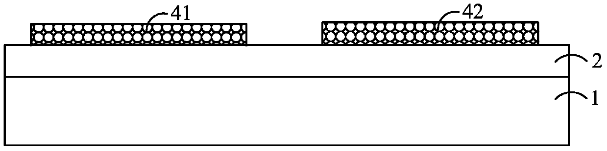
[0031] Such as figure 2 As shown, a glass substrate 1 is provided, and a buffer layer 2 and an amorphous silicon layer 31 are sequentially deposited on the glass substrate 1 by chemical vapor deposition (CVD, Chemical Vapor Deposition), wherein the buffer layer is a silicon nitride layer. Using excimer laser annealing (ELA, Excimer Laser Annel) or solid phase crystallization (SPC, Solid Phase Crystallization) method to transform the amorphous silicon layer 3 into a polysilicon layer, and then define the polysilicon layer by photolithography and etching processes such as image 3 In the two polysilicon island patterns shown, the two polysilicon islands are the active layers, the one on the left is the first active layer 41 , and the one on the right is the second active layer 42 .

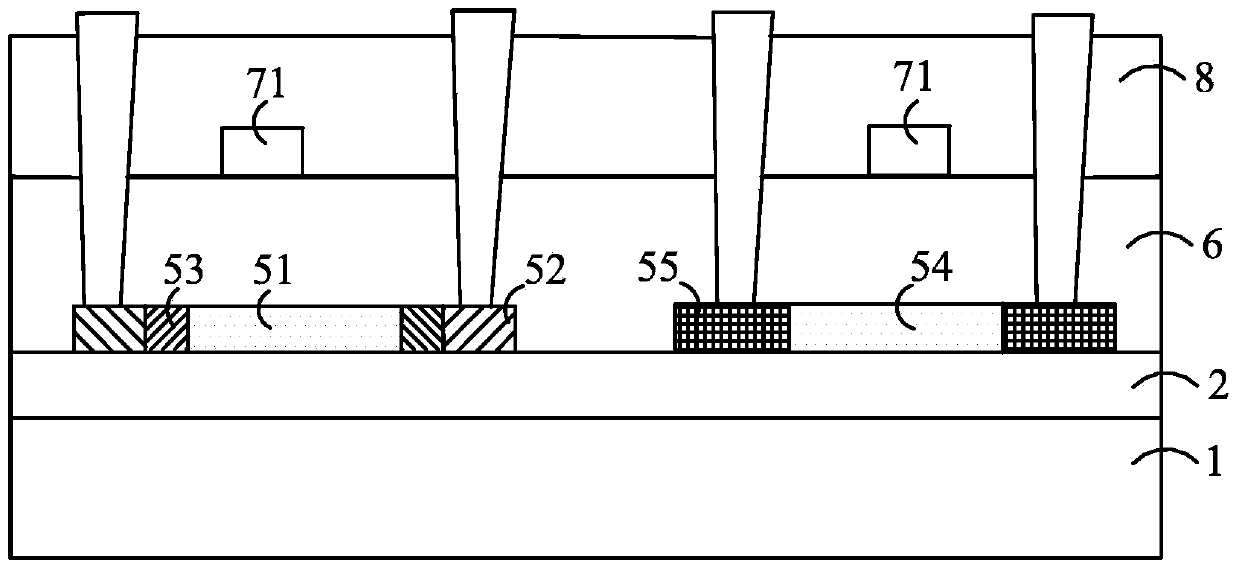
[0032] Next, if Figure 4 As shown, the first channel 51 , the N+ r...


PUM


Abstract

The invention relates to a low-temperature polycrystalline silicon thin film transistor and a preparation method thereof. The method comprises the following steps: providing a substrate; depositing a buffering layer and a non-crystalline silicon layer on the substrate in sequence, and performing laser radiation to change the non-crystalline silicon layer into a polycrystalline silicon layer which is an active layer; depositing a first grid insulating layer, a second grid insulating layer and a first metal layer on the buffering layer and the active layer in sequence, performing high-temperature activation, and photoetching and etching the first metal layer to form a grid; depositing dielectric layers on the grid insulating layers and the grid; depositing first contact holes and second contact holes in the dielectric layers, the first grid insulating layer and the second grid insulating layer; and respectively depositing source electrodes and drain electrodes on the first contact holes and the second contact holes. The thin film transistor prepared by the method can effectively overcome the structural defects of polycrystalline silicon, and the performance of the thin film transistor can be improved.

Description

technical field [0001] The invention relates to the field of display technology, in particular to a low-temperature polysilicon thin film transistor and a manufacturing method thereof. Background technique [0002] Thin Film Transistor (TFT, Thin Film Transistor) is used as a switching element in liquid crystal display devices. It has the characteristics of low power consumption, small volume and low driving voltage, and is very suitable for computers, notebooks and other devices. display screen. In the current liquid crystal display device, the active layer of the thin film transistor is mainly made of amorphous silicon (a-Si), but the mobility of the thin film transistor using amorphous silicon as the active layer is very low, and it is difficult to meet the driving requirements of the peripheral circuit. Therefore, the technology of using low temperature polysilicon (Low Temperature Poly-silicon, LTPS) instead of amorphous silicon emerges as the times require. [0003] ...

Claims


Application Information

Patent Timeline
Patent Type & Authority Patents(China)
IPC IPC(8): H01L29/786H01L29/423H01L21/336
CPCH01L29/42364H01L29/66757H01L29/78675H01L2029/42388
Inventor 张占东
Owner WUHAN CHINA STAR OPTOELECTRONICS TECH CO LTD
Why Eureka
Try Eureka