Passivation layer deposition method of high-voltage LED chip

A technology of LED chips and deposition methods, applied in electrical components, circuits, semiconductor devices, etc., can solve the problems affecting the yield rate of high-voltage LED chips, broken bridges, etc., to reduce the tilt angle, avoid bridge breakage, and improve yield. Effect

Active Publication Date: 2016-06-08
BEIJING NAURA MICROELECTRONICS EQUIP CO LTD
View PDF9 Cites 6 Cited by
  • Summary
  • Abstract
  • Description
  • Claims
  • Application Information

AI Technical Summary

Problems solved by technology

[0010] In the actual production process, bridge breakage often occurs when evaporating electrode connection bridges, which affects the yield of high-voltage LED chips. The side wall is relatively steep, which makes it impossible for the electrode connection bridge 7 to "climb" to the slightly higher P electrode during the process of evaporating the electrode connection bridge 7

Method used


Image

  • Passivation layer deposition method of high-voltage LED chip
  • Passivation layer deposition method of high-voltage LED chip
  • Passivation layer deposition method of high-voltage LED chip

Examples


Embodiment Construction

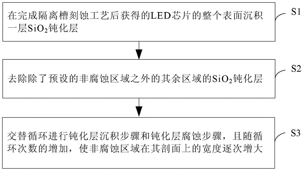
[0035] In order to enable those skilled in the art to better understand the technical solution of the present invention, the method for etching isolation grooves of GaN-based LED chips provided by the present invention will be described in detail below with reference to the accompanying drawings.

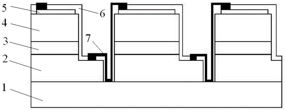
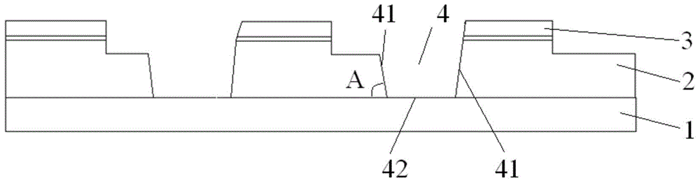
[0036] The passivation layer deposition method of the high-voltage LED chip provided by the present invention is carried out after the etching process of the isolation groove and before the evaporation process of the electrode connecting bridge, so as to deposit SiO on the surface of the LED chip. 2 passivation layer. After the etching process of the isolation groove is completed, the side wall of the isolation groove obtained is relatively steep, which makes it impossible for the electrode connection bridge to "climb" to the P electrode with a slightly higher height during the process of evaporating the electrode connection bridge, so that it is often There is a broken bridge. Thi...


PUM


Abstract

The invention provides a passivation layer deposition method of a high-voltage LED chip. The method comprises the following steps: a passivation layer deposition step, i.e., depositing an SiO2 passivation layer on the whole surface of an LED chip obtained after an isolation groove etching process is completed; a passivation layer removing step, i.e., removing the SiO2 passivation layer of other areas apart from a preset non-corrosion area, wherein the non-corrosion area comprises the side wall of an isolation groove and an area, adjacent to the side wall, of the bottom surface of the isolation groove; and alternatively performing the passivation layer deposition step and the passivation layer removing step for multiple times, and enabling the width of the non-corrosion area on a profile to be successively increased as the alternating frequency increases. According to the passivation layer deposition method of the high-voltage LED chip, provided by the invention, the inclination angle of the side wall of the chip can be reduced, bridge disconnection can be prevented during vapor plating of an electrode connection bridge, and accordingly, the yield rate of the high-voltage LED chip can be improved.

Description

technical field [0001] The invention relates to the technical field of semiconductor processing, in particular to a high-voltage LED core [0002] Chip passivation layer deposition method. Background technique [0003] Light Emitting Diode (LED) is gradually becoming the mainstream lighting source in the traditional lighting market due to its advantages of high luminous efficiency, low energy consumption, long life, and non-toxic green. Many applications. High-Voltage LED (High-Voltage LED) has gradually become a new breakthrough in the lighting field due to its advantages of small current drive and simple drive circuit design. In a broad sense, high-voltage LED refers to the method of dividing the epitaxial layer of a large-size chip (generally 45*45mil) into multiple independent core particles by etching deep trenches, and connecting bridges through evaporation electrodes. The LED chip formed by connecting each chip in series, because the voltage of a single chip is 3V ...

Claims


Application Information

Patent Timeline
Patent Type & Authority Applications(China)
IPC IPC(8): H01L33/00H01L33/36
Inventor 李航
Owner BEIJING NAURA MICROELECTRONICS EQUIP CO LTD
Why Eureka
Try Eureka