Method of etching polycrystalline silicon sheet cut by diamond wire
A technology of diamond wire cutting and polysilicon wafers, which is applied in the fields of chemical instruments and methods, crystal growth, and final product manufacturing. It can solve the problems of low reflectivity and low conversion efficiency, improve conversion efficiency, save costs, and simplify process operations. Effect
- Summary
- Abstract
- Description
- Claims
- Application Information
AI Technical Summary
Problems solved by technology
Method used
Image

Examples
Embodiment 1
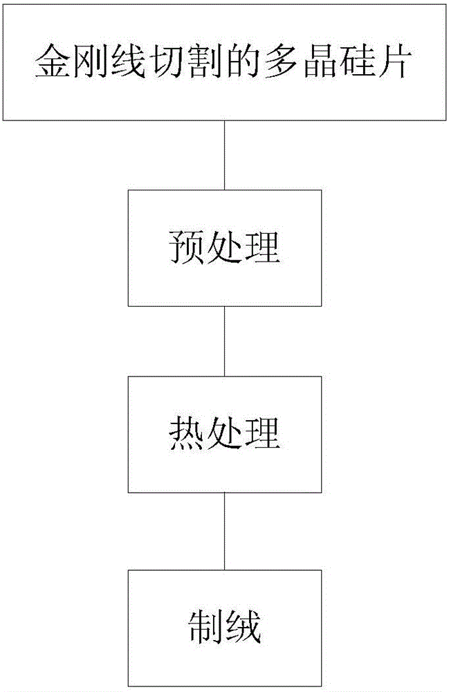
[0024] Such as figure 1 Shown, a kind of method for making texture of diamond wire-cut polysilicon wafer, comprises the following steps:
[0025] Step 1): pretreatment, cleaning the polysilicon wafer cut by diamond wire, and drying after cleaning; wherein, the cleaning in the step 1) is RCA solution cleaning, and the NH in the RCA solution 4 OH, H 2 o 2 、H 2 The volume ratio of O is 1:1:5; the drying in the step 1) is specifically: the water on the surface of the silicon wafer is removed by the surface tension of the DI water with high cleanliness (the resistivity is greater than 16MΩ) after heating. The top of the polysilicon wafer is dried by blowing clean air at 80°C downward.
[0026] Step 2): heat treatment, performing heat treatment on the polycrystalline silicon wafer treated in the step 1); wherein, the heating temperature of the heat treatment in the step 2) is 700° C., and the heating time is 50 s.
[0027] Step 3): Texturing, putting the polycrystalline silicon...
Embodiment 2
[0029] Such as figure 1 Shown, a kind of method for making texture of diamond wire-cut polysilicon wafer, comprises the following steps:
[0030] Step 1): pretreatment, cleaning the polysilicon wafer cut by diamond wire, and drying after cleaning; wherein, the cleaning in the step 1) is RCA solution cleaning, and the NH in the RCA solution 4 OH, H 2 o 2 、H 2The volume ratio of O is 1:1:5; the drying in the step 1) is specifically: the water on the surface of the silicon wafer is removed by the surface tension of the DI water with high cleanliness (the resistivity is greater than 16MΩ) after heating. The top of the polysilicon wafer is blown down with clean air at 90°C for drying.
[0031] Step 2): heat treatment, performing heat treatment on the polycrystalline silicon wafer treated in the step 1); wherein, the heating temperature of the heat treatment in the step 2) is 900° C., and the heating time is 600 s.
[0032] Step 3): Texturing, putting the polycrystalline silico...
Embodiment 3
[0034] Such as figure 1 Shown, a kind of method for making texture of diamond wire-cut polysilicon wafer, comprises the following steps:
[0035] Step 1): pretreatment, cleaning the polysilicon wafer cut by diamond wire, and drying after cleaning; wherein, the cleaning in the step 1) is RCA solution cleaning, and the NH in the RCA solution 4 OH, H 2 o 2 、H 2 The volume ratio of O is 1:1:5; the drying in the step 1) is specifically: the water on the surface of the silicon wafer is removed by the surface tension of the DI water with high cleanliness (the resistivity is greater than 16MΩ) after heating. The top of the polysilicon wafer is dried by blowing clean air at 95°C downward.
[0036] Step 2): heat treatment, performing heat treatment on the polycrystalline silicon wafer treated in the step 1); wherein, the heating temperature of the heat treatment in the step 2) is 800° C., and the heating time is 300 s.
[0037] Step 3): Texturing, putting the polycrystalline silico...
PUM
| Property | Measurement | Unit |
|---|---|---|
| thickness | aaaaa | aaaaa |
| reflectance | aaaaa | aaaaa |
Abstract
Description
Claims
Application Information
 - R&D
- Intellectual Property
- Life Sciences
- Materials
- Tech Scout
- Unparalleled Data Quality
- Higher Quality Content
- 60% Fewer Hallucinations
Browse by: Latest US Patents, China's latest patents, Technical Efficacy Thesaurus, Application Domain, Technology Topic, Popular Technical Reports.
© 2025 PatSnap. All rights reserved.Legal|Privacy policy|Modern Slavery Act Transparency Statement|Sitemap|About US| Contact US: help@patsnap.com