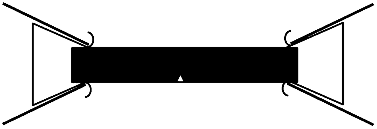
A kind of brittle fracture method of flexible film
A flexible film and brittle fracture technology, applied in the field of scanning electron microscope sample preparation, can solve the problems of plastic deformation, insufficient liquid nitrogen precooling, loss, etc.
- Summary
- Abstract
- Description
- Claims
- Application Information
AI Technical Summary
Problems solved by technology
Method used
Image
Examples
Embodiment 1
[0034] Taking the preparation of the brittle section of a polymer flexible film for scanning electron microscopy as an example, the flexible film is a SPEEK proton exchange membrane.
[0035] First, like figure 1 As shown, prepare a long silicon wafer with a length of 1.5 cm, a width of 5 mm, and a length-to-width ratio far greater than 2:1, which meets the restriction conditions, and then use a glass knife on the side of the middle of the silicon wafer. Carved, a silicon wafer with grooves on one side is obtained.
[0036] Then prepare the flexible film, and cut the polymer flexible film into a size slightly smaller than the long silicon wafer. The length is 1cm and the width is 3mm.
[0037] The third step, such as figure 2 As shown, the polymer flexible film, the carbon conductive double-sided tape, and the silicon wafer are sequentially pasted into a sandwich structure to form a composite silicon wafer. The silicon wafer is the lowermost layer and the grooved surface is facing ...
Embodiment 2
[0042] Take the preparation of the brittle section of a polymer flexible film for scanning electron microscopy as an example. The flexible film is a lithium battery separator, made of polypropylene, and has many microporous structures. It is easy to form closed cells by ordinary methods.
[0043] First, like figure 1 As shown, prepare a long silicon wafer with a length of 1.5 cm and a width of 5 mm, and then use a glass knife to pre-engrave the middle side of the silicon wafer to obtain a silicon wafer with grooves on one side.
[0044] Then prepare a flexible film, and cut the polymer flexible film into a size similar to a long silicon wafer with a length of 1 cm and a width of 3 mm.
[0045] The third step, such as figure 2 As shown, the polymer flexible film, the carbon conductive double-sided tape, and the silicon wafer are sequentially pasted into a sandwich structure to form a composite silicon wafer. The silicon wafer is the lowermost layer and the grooved surface is facing d...
Embodiment 3
[0050] Taking the preparation of the brittle section of a polymer flexible film for scanning electron microscopy as an example, the flexible film is a polyethylene cling film made of polypropylene, which is relatively flexible at low temperatures.
[0051] First, like figure 1 As shown, prepare a long silicon wafer with a length of 1.5 cm and a width of 5 mm, and then use a glass knife to pre-engrave the middle side of the silicon wafer to obtain a silicon wafer with grooves on one side.
[0052] Then prepare the flexible film, and cut the polymer flexible film into a size similar to the long silicon wafer, with a length of 1 cm and a width of 3 mm.
[0053] In the third step, because the polyethylene cling film is still very tough at the temperature of liquid nitrogen, the above sandwich structure is strengthened, and the pre-grooved silicon wafer, carbon conductive double-sided tape, polymer flexible film, and carbon conductive double-sided tape The silicon wafers are sequentially...
PUM
| Property | Measurement | Unit |
|---|---|---|
| thickness | aaaaa | aaaaa |
| boiling point | aaaaa | aaaaa |
Abstract
Description
Claims
Application Information


