Non-contact silicon chip deformation compensation apparatus and method based on electrostatic effect

A deformation compensation device and non-contact technology, applied in the field of integrated circuit equipment manufacturing, can solve the problems of inability to solve the deformation of the silicon wafer itself and clamping deformation, unfavorable overlay and focal plane error, uncontrollable local deformation amount, etc. Eliminate thermal deformation effects, avoid contact contamination, improve productivity

Active Publication Date: 2016-06-29
SHANGHAI MICRO ELECTRONICS EQUIP (GRP) CO LTD
View PDF7 Cites 2 Cited by
  • Summary
  • Abstract
  • Description
  • Claims
  • Application Information

AI Technical Summary

Problems solved by technology

However, this solution can only solve the thermal deformation of the silicon wafer, and cannot solve the self-deformation and clamping deformation of the silicon wafer.
In addition, since ASML's current mainstream lithography equipment is a dual-stage architecture (such as NXT1950I), that is, only the measurement end of the "dry" environment is used to measure the topography of the silicon wafer, while the local shape caused by the exposure end of the "wet" environment Variables cannot be controlled and eliminated, which obviously does not take advantage of further control of overlay and focal plane errors

Method used


Image

  • Non-contact silicon chip deformation compensation apparatus and method based on electrostatic effect
  • Non-contact silicon chip deformation compensation apparatus and method based on electrostatic effect
  • Non-contact silicon chip deformation compensation apparatus and method based on electrostatic effect

Examples


Embodiment Construction

[0025] Specific embodiments of the present invention will be described in detail below in conjunction with the accompanying drawings.

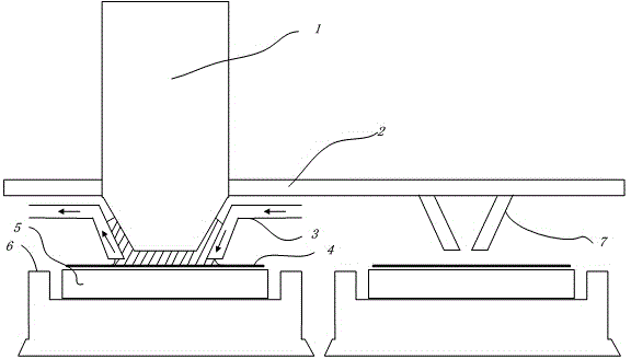
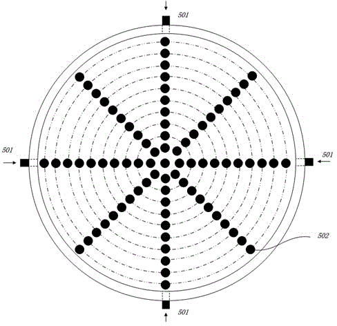
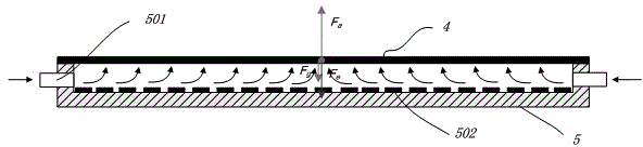
[0026] The present invention discloses a non-E-PIN type silicon chip clamping and surface compensation device coupled with positive air flotation and non-contact electrostatic adsorption, so as to eliminate contact pollution, and can monitor and adjust the local surface shape of silicon chips in real time , to eliminate the deformation of the silicon wafer itself and the clamping deformation. The technical solution provided by the present invention can further couple the local temperature measurement of the silicon wafer and the compensation electrode array together, and can further eliminate the influence of the thermal deformation of the silicon wafer, thereby optimizing the effect of the deformation of the silicon wafer introduced by the immersion flow field on overlaying and focusing. Deep impact, and can avoid the continuous leveling and ...


PUM


Abstract

The invention discloses a non-contact silicon chip deformation compensation apparatus, comprising a forward air floatation unit and an electrostatic adsorption unit, wherein the forward air floatation unit comprises a shell and a groove, a stationary electrode array is arranged at the bottom of the inner side of the groove, and the forward air floatation unit further comprises a plurality of air inlets formed in the shell an used for guiding in compressed air.

Description

technical field [0001] The invention relates to the field of integrated circuit equipment manufacturing, in particular to a non-contact silicon wafer deformation compensation device and method based on electrostatic effects. Background technique [0002] 193nm immersion lithography technology is currently the mainstream lithography technology for nodes below 45nm. It introduces a liquid with a high refractive index n (such as deionized water, etc.) between the lower surface of the objective lens and the photoresist on the silicon wafer. Increase the numerical aperture of the objective lens (N.A.>1.3) to greatly improve the resolution and increase the depth of focus. The research shows that the deformation of the silicon wafer mainly comes from: (1) the flatness error of the silicon wafer material itself; (2) the clamping deformation of the silicon wafer; (3) the thermal deformation of the silicon wafer. [0003] As for the flatness error of the silicon wafer material its...

Claims


Application Information

Patent Timeline
Patent Type & Authority Applications(China)
IPC IPC(8): G03F7/20
Inventor 朱树存丁姗
Owner SHANGHAI MICRO ELECTRONICS EQUIP (GRP) CO LTD
Why Eureka
Try Eureka