Pixel circuit based on double-gate transistor and drive method thereof

A technology of double-gate transistors and pixel circuits, which can be used in instruments, static indicators, etc., and can solve problems such as uneven pixel matrix display, long set-up time, and component aging

Active Publication Date: 2016-07-06
PEKING UNIV SHENZHEN GRADUATE SCHOOL
View PDF9 Cites 49 Cited by
  • Summary
  • Abstract
  • Description
  • Claims
  • Application Information

AI Technical Summary

Problems solved by technology

[0005] Although figure 1 The structure of the pixel circuit shown is simple, but as time goes by, the components in it will age, especially the drive transistor T1 and the organic light-emitting diode OLED will age, resulting in drift in the threshold voltage of the drive transistor T1 and OLED, and the pixel matrix The threshold voltage drift of the drive transistor T1 and OLED of each pixel unit in the pixel matrix is ​​also different; in addition, because the thin film field effect transistor is made of polysilicon material, the threshold voltage of the drive transistor T1 of each pixel unit in the pixel matrix will be V TH It has non-uniform characteristics; in the above two cases, according to the formula (1), it can be seen that the drivi

Method used


Image

  • Pixel circuit based on double-gate transistor and drive method thereof
  • Pixel circuit based on double-gate transistor and drive method thereof
  • Pixel circuit based on double-gate transistor and drive method thereof

Examples


Embodiment 1

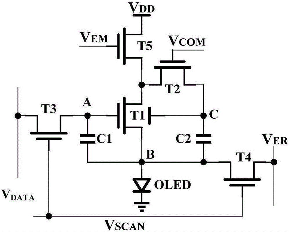
[0071] Please refer to figure 2 This embodiment proposes a pixel circuit based on double-gate transistors (hereinafter referred to as the pixel circuit), which includes a light emitting device OLED, a driving transistor T1, switching transistors T2-T5, and capacitors C1 and C2, which will be described in detail below.

[0072] The anode of the light emitting device OLED is connected to an internal node B, and the cathode of the light emitting device OLED is connected to a low level line V SS . The light emitting device OLED is used to display relevant image or video information.

[0073] The driving transistor T1 is a double-gate transistor, and is used to drive the light emitting device OLED to emit light, that is, to provide pixel current for the light emitting device OLED. In one embodiment, the driving transistor T1 is a dual-gate a-IGZO transistor. The bottom gate of the driving transistor T1 is connected to an internal node A, the top gate of the driving transistor T...

Embodiment 2

[0090] In the driving method provided by Embodiment 1, in each frame, all pixel circuits sequentially perform the above initialization step S01, threshold voltage extraction step S03, data writing step S05 and light emitting step S07. Considering that after each extraction of the threshold voltage is completed, since the capacitor C2 stores the top gate source voltage of the driving transistor T1, the threshold voltage will be stored for a period of time, and there is no need to extract the threshold value when the next frame is refreshed Voltage, just complete data writing and subsequent light emission.

[0091] This embodiment proposes a driving method including the pixel circuit in the first embodiment, which is used for a pixel matrix including several pixel circuits. In an embodiment, in the pixel matrix including the above pixel circuits, all the pixel circuits can share the same fixed level line V ER , the same light-emitting control line V EM and the same threshold e...

Embodiment 3

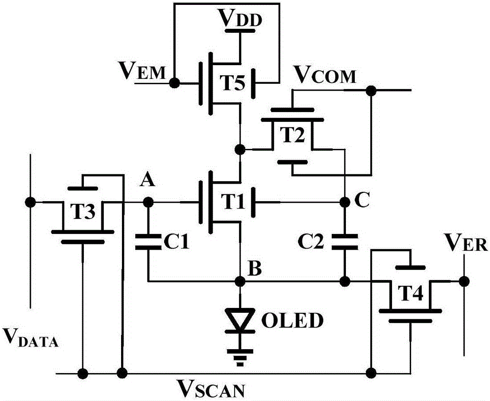
[0104] This implementation proposes a pixel circuit based on double-gate transistors. The difference from the pixel circuit of the embodiment is that the pixel circuit of this embodiment adds a switching transistor T6, which replaces the switching transistor T3 in the first embodiment, and is used to transfer The voltage VREF is given to the internal node A, so that the switching transistor T3 only needs to pass the voltage V containing the display data DATA , so that the initialization step and the threshold value extraction step do not need to occupy the line time, thereby improving the driving speed while obtaining a better compensation effect.

[0105] Please refer to Figure 8 , which is the pixel circuit of this embodiment, compared with figure 2 In the pixel circuit shown in Embodiment 1, the pixel circuit of this embodiment adds a switch transistor T6, wherein the gate of the switch transistor T6 is connected to the threshold value extraction control line V COM , th...


PUM


Abstract

The application discloses a pixel circuit based on a double-gate transistor and a drive method thereof. In one embodiment, the pixel circuit comprises a light-emitting device OLED, a drive transistor T1, switch transistors T2-T5, a capacitor C1 and a capacitor C2; and the drive transistor T1 is a double-gate transistor and is used to drive the light-emitting device OLED to emit light. For the drive transistor in the pixel circuit of the application, the double-gate transistor is used to replace a single-gate transistor as a drive transistor in a traditional technology, a bottom gate of the double-gate transistor is used as the main gate, and then a top gate source voltage is used to adjust a threshold voltage of the drive transistor; and, because stability of a double-gate a-IGZO TFT is higher than stability of a single-gate device, the double-gate a-IGZO TFT can achieve threshold extraction and compensation and can achieve good display uniformity at the same time.

Description

technical field [0001] The present application relates to the technical field of displays, in particular to a pixel circuit based on a double-gate transistor and a driving method thereof. Background technique [0002] Active matrix organic light-emitting diode (Active Matrix Organic Light-Emitting Diode, OLED) has been widely studied in recent years due to its advantages of high brightness, high luminous efficiency, wide viewing angle and low power consumption, and has been rapidly applied to a new generation of display systems. . The traditional AMOLED pixel unit is a structure of two thin film field effect transistors (ThinFilmTransistor, TFT) and a storage capacitor, such as figure 1 As shown, where T1 is the driving transistor, T2 is the switching transistor, C S For storage capacitors and OLEDs for light emitting devices. The switching transistor T2 responds to the signal from the scan control signal line, samples the signal from the data line, and the storage capaci...

Claims


Application Information

Patent Timeline
IPC IPC(8): G09G3/3233
CPCG09G3/3233
Inventor 张盛东王翠翠
Owner PEKING UNIV SHENZHEN GRADUATE SCHOOL
Why Eureka
Try Eureka