Light emitting diode and manufacturing method therefor

A technology of light-emitting diodes and manufacturing methods, which is applied in the direction of electrical components, circuits, semiconductor devices, etc., can solve the problems of uneven light extraction efficiency, poor antistatic ability of LEDs, and low light extraction efficiency, so as to reduce the carrier aggregation effect and improve The effect of LED reliability and enhanced light extraction efficiency

Active Publication Date: 2016-07-06
TIANJIN SANAN OPTOELECTRONICS
View PDF6 Cites 0 Cited by
  • Summary
  • Abstract
  • Description
  • Claims
  • Application Information

AI Technical Summary

Problems solved by technology

[0002] Light Emitting Diode (English for LightEmittingDiode, abbreviated as LED) is a semiconductor solid-state light-emitting device, which uses a semiconductor PN junction as a light-emitting structure. Gallium nitride is currently regarded as the third-generation III-IV semiconductor with a wide band gap and high luminescence. Efficiency, stable chemical properties, etc., but the LED with traditional epitaxial structure has poor antistatic ability and uneven light output efficiency due to the current congestion phenomenon under the P electrode.
[0003] In the design of LED structure, the solutions given for uneven luminescence, low light extraction efficiency and poor antistatic ability are to deposit a transparent current spreading layer (such as ITO) on the contact layer by chip technology, or on the P-type However, the above structures all achieve a certain degree of current expansion through the free distribution of carriers on the contact surface of the insertion layer or inside the insertion layer.

Method used


Image

  • Light emitting diode and manufacturing method therefor

Examples


Embodiment

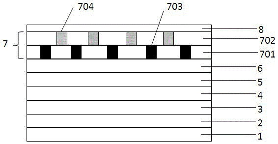
[0017] figure 1 It is a schematic diagram of the structure of a light-emitting diode epitaxial wafer implemented according to the present invention. In this embodiment, the epitaxial layer includes from bottom to top: (1) sapphire substrate 1; (2) low-temperature buffer layer 2, which can be gallium nitride, nitrogen Aluminum oxide, or aluminum-gallium-nitride combination, with a film thickness between 10 and 100 μm; (3) non-doped gallium nitride layer 3, with a film thickness between 300 and 7000 μm, preferably 3500 μm; (4) N-type gallium nitride layer 4. The thickness is greater than 1 μm; (5) The quantum well light-emitting layer 5 is composed of InGaN as the well layer and GaN or AlGaN or a combination of the two as the barrier layer, wherein the thickness of the barrier layer is between 50 and 150 nm, and the thickness of the well layer is 1 ~20nm; (6) P-type layer 6, thickness between 0.05-1μm; (7) insertion layer 7; (8) contact layer 8, thickness between 0.1nm~20nm.

...


PUM


Abstract

The invention provides a light emitting diode and a manufacturing method therefor. The light emitting diode comprises an N type layer, a light emitting layer, a P type layer and a contact layer, wherein an insertion layer is designed between the P type layer and the contact layer; the insertion layer comprises an N<+> nitride layer and a P<+> nitride layer which are disjunctively distributed in a doping region; and the N<+> nitride layer and the P<+> nitride layer are not fully overlapped in the doping region in a perpendicular direction. Inclined tunneling junctions are formed by the N<+> nitride layer and the P<+> nitride layer disjunctively distributed in the doping region in the insertion layer, so that the current expansion is reinforced, and the luminance and reliability of the LED are improved.

Description

technical field [0001] The invention relates to the field of gallium nitride semiconductor devices, in particular to a light emitting diode with an effective current spreading layer and a manufacturing method thereof. Background technique [0002] Light Emitting Diode (English for LightEmittingDiode, abbreviated as LED) is a semiconductor solid-state light-emitting device, which uses a semiconductor PN junction as a light-emitting structure. Gallium nitride is currently regarded as the third-generation III-IV semiconductor with a wide band gap and high luminescence. Efficiency, stable chemical properties, etc., but the LED with the traditional epitaxial structure has poor antistatic ability and uneven light output efficiency due to the current congestion phenomenon under the P electrode. [0003] In the design of LED structure, the solutions given for uneven luminescence, low light extraction efficiency and poor antistatic ability are to deposit a transparent current spreadi...

Claims


Application Information

Patent Timeline
IPC IPC(8): H01L33/04H01L33/32H01L33/00
CPCH01L33/0062H01L33/04H01L33/32
Inventor 舒立明叶大千刘晓峰高文浩王良均吴超瑜王笃祥
Owner TIANJIN SANAN OPTOELECTRONICS
Why Eureka
Try Eureka