Flash memory storage unit and manufacturing method therefor

A manufacturing method and flash memory storage technology, which are applied in the fields of electrical components, semiconductor/solid-state device manufacturing, semiconductor devices, etc., can solve the problems of high device power consumption, low effective coupling capacitance between floating gate and control gate, and failure, and reduce power consumption. consumption, improve the effect of erasing and writing speed and reliability

Active Publication Date: 2016-07-20
GIGADEVICE SEMICON SHANGHAI INC +1
View PDF6 Cites 0 Cited by
  • Summary
  • Abstract
  • Description
  • Claims
  • Application Information

AI Technical Summary

Problems solved by technology

[0004] The method for making the above-mentioned flash memory storage unit has the following disadvantages: due to the instability of the etched shape of the silicon nitride layer, it is easy to cause process defects such as filling gaps in the floating gate when filling the floating gate, and this method fills the gap between the formed floating gate and the control gate. The contact area A is small, resulting in low effective coupling capacitance between the floating gate and the control gate, and the distance between the control gate and the active area is relatively close, and the parasitic coupling capacitance between the control gate and the active area is relatively high, so that the control gate cannot effectively control The opening and closing of the floating gate device causes high power consumption or even failure of the device

Method used


Image

  • Flash memory storage unit and manufacturing method therefor
  • Flash memory storage unit and manufacturing method therefor
  • Flash memory storage unit and manufacturing method therefor

Examples


Embodiment 1

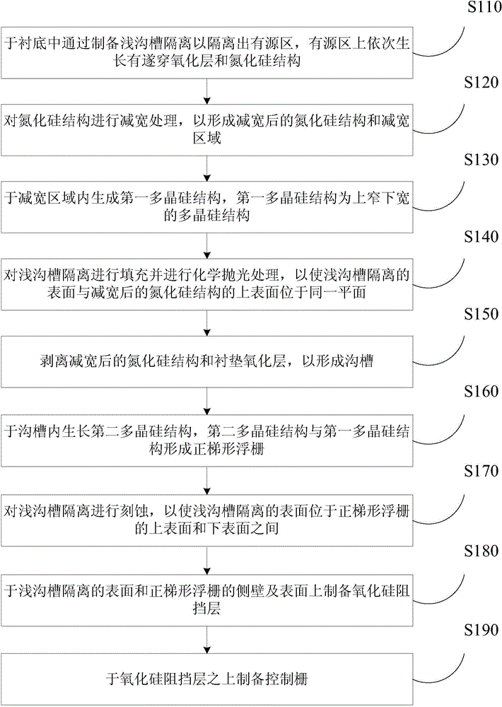
[0057] figure 2A flow chart of the method for manufacturing a flash storage unit provided in Embodiment 1 of the present invention is given. Such as figure 2 As shown, the method for manufacturing a flash memory storage unit provided in Embodiment 1 includes the following steps:

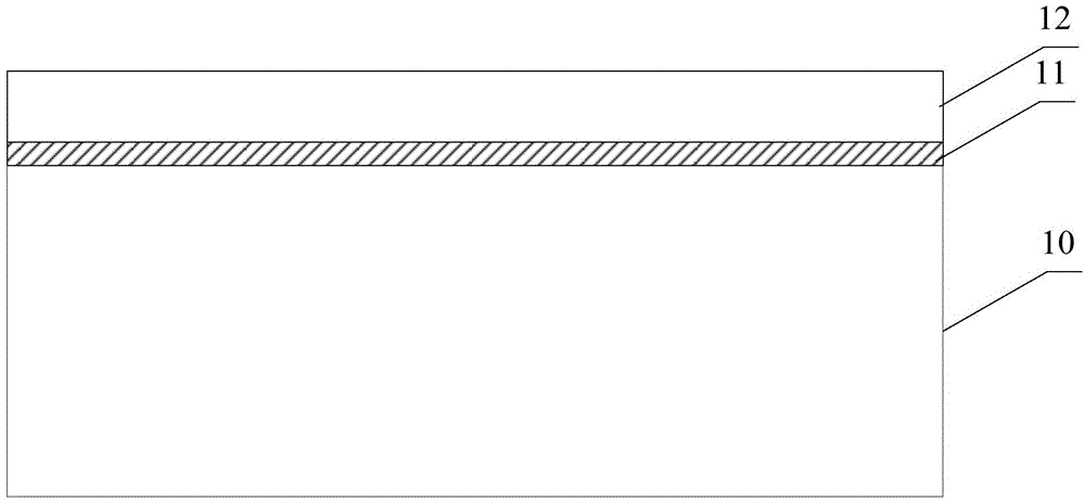
[0058] Step S110, isolating the active region 15 by preparing shallow trench isolation 14 in the substrate 10, on which the tunneling oxide layer 11 and the silicon nitride structure 12a are sequentially grown;

[0059] Specifically, such as Figure 3 to Figure 6 shown, refer to image 3 Firstly, a tunnel oxide layer 11 and a silicon nitride layer 12 are sequentially grown on the substrate 10, wherein the substrate 10 can be a silicon substrate, a silicon germanium substrate, a germanium substrate or a III-V compound substrate, In this embodiment, the substrate 10 is taken as a silicon substrate as an example. The material of the tunnel oxide layer 11 is preferably silicon oxide, and ion impla...

Embodiment 2

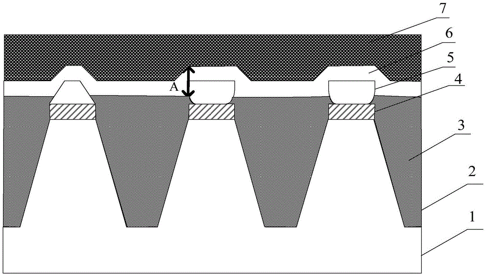
[0079] This embodiment provides a flash storage unit, such as Figure 16 shown, including:

[0080] a substrate 10, the upper part of the substrate 10 is formed with a plurality of shallow trenches 13;

[0081] tunneling the oxide layer 11, grown on the substrate 10;

[0082] a positive trapezoidal floating gate 19 formed on the tunnel oxide layer 11;

[0083] Shallow trench isolation 14, formed in the plurality of shallow trenches 13 and on the sidewalls of the positive trapezoidal floating gate 19;

[0084] a silicon oxide blocking layer 20 formed on the surface of the shallow trench isolation 14 and the sidewall and surface of the positive trapezoidal floating gate 19;

[0085] The control gate 21 is formed on the silicon oxide blocking layer 20 .

[0086] The flash memory storage unit provided in this embodiment uses floating gate etching technology to produce a positive trapezoidal floating gate structure. Due to the stability of the positive trapezoidal floating gate...


PUM

PropertyMeasurementUnit
thicknessaaaaaaaaaa
thicknessaaaaaaaaaa

Abstract

The invention discloses a flash memory storage unit and a manufacturing method therefor. The manufacturing method comprises the steps of forming an active region in a substrate by preparing a shallow trench isolation part in an isolation manner, wherein a tunneling oxide layer and a silicon nitride structure are grown on the active region in sequence; reducing the width of the silicon nitride structure to form a narrowed silicon nitride structure and a narrowing region; preparing a first polysilicon structure in the narrowing region; filling the shallow trench isolation part; peeling off the narrowed silicon nitride structure to form a trench; enabling a second polysilicon structure to be grown in the trench, wherein a regular trapezoidal floating gate is formed by the second polysilicon structure and the first polysilicon structure; etching the shallow trench isolation part; preparing a silicon oxide barrier layer on the surface of the shallow trench isolation part and the side wall and the surface of the regular trapezoidal floating gate; and preparing a control gate on the silicon oxide barrier layer. The manufacturing method for the flash memory storage unit has the beneficial effects of lowering the power consumption of the floating gate device, and improving the erasing speed and reliability of the flash memory storage.

Description

technical field [0001] The invention relates to the field of manufacturing semiconductor devices, in particular to a flash memory storage unit and a manufacturing method. Background technique [0002] Flash memory (Flash Memory, referred to as flash memory) is a long-life non-volatile semiconductor memory that can still maintain stored data information in the event of a power failure. It is widely used in USB flash drives, flash memory cards, and notebook computers. , And digital cameras, mobile phones and other portable flash memory digital storage products. [0003] The prior art provides a method for manufacturing a flash memory unit. First, an oxide layer and a silicon nitride layer are sequentially formed on a substrate 1, and the oxide layer and the silicon nitride layer are used as a hard mask layer; Etching shallow trenches 2 arranged in parallel on the substrate 1 with a hard film layer, and forming a regular trapezoidal silicon nitride structure and a silicon nitr...

Claims


Application Information

Patent Timeline
Patent Type & Authority Applications(China)
IPC IPC(8): H01L27/115H01L21/8247
Inventor 刘钊熊涛许毅胜舒清明
Owner GIGADEVICE SEMICON SHANGHAI INC
Why Eureka
Try Eureka