Trench gate insulated gate bipolar transistor (IGBT) device and manufacturing method thereof

A trench gate and device technology, applied in the field of implant enhanced trench gate insulated gate bipolar transistor and insulated gate bipolar transistor, achieves good forward conduction voltage drop, good switching loss, and improved carrier concentration distribution Effect

Active Publication Date: 2016-07-20
UNIV OF ELECTRONICS SCI & TECH OF CHINA
View PDF5 Cites 16 Cited by
  • Summary
  • Abstract
  • Description
  • Claims
  • Application Information

AI Technical Summary

Problems solved by technology

The present invention introduces an electrode connected to the emitter at the bottom of the gate electrode of the IEGT device through the introduction of the mutually coupled composite trench structure and the carrier storage layer. The depth and width of the electrode, on the other hand, reduces the gate capacitance of the device, especially the gate-collector capacitance, by introducing the shielding effect of the electrode connected to the emitter, increasing the switching speed of the device and reducing the switching speed of the device. At the same time, the introduction of the coupled carrier storage layer compensates for the adverse effect on the forward conduction characteristics of the device due to the introduction of the lower gate electrode connected to the emitter, further improving the carrier concentration distribution in the entire drift region, and obtaining A better compromise between the device forward voltage drop and switching loss; in addition, the thick dielectric layer around the bottom electrode further shields the adverse effect of the N-type charge storage layer on the device breakdown voltage, and in a certain device trench In the case of groove depth and trench MOS structure density, the breakdown voltage of the device is further improved, the concentration of the electric field at the bottom of the trench is improved, and the reliability of the device is further improved

Method used


Image

  • Trench gate insulated gate bipolar transistor (IGBT) device and manufacturing method thereof
  • Trench gate insulated gate bipolar transistor (IGBT) device and manufacturing method thereof
  • Trench gate insulated gate bipolar transistor (IGBT) device and manufacturing method thereof

Examples


Embodiment 1

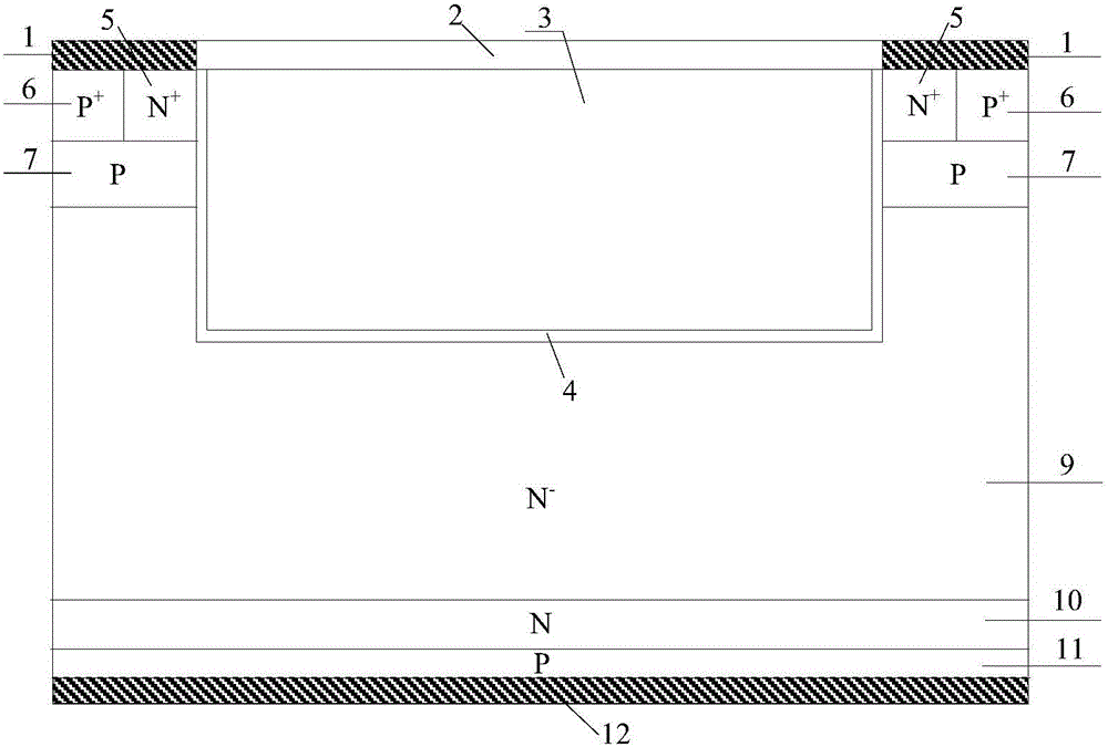
[0042] The trench gate IGBT of this example has a cell structure such as figure 2 As shown, it includes: a back collector metal 12, a P-type collector region 11 located on and connected to the back collector metal 12, an N-type field stop layer 10 located on and connected to the P-type collector region 11, The N-drift region 9 located on the N-type field stop layer 10 and connected to it; the composite trench structure located in the middle of the upper part of the N-drift region 9 and connected to it; The p-type body region 7, the sidewalls of the p-type body region 7 are connected to the sidewalls of the composite trench structure; the independent N+ emitter region 5 and the P+ emitter region 6 located on the upper part of the p-type body region 7 and connected thereto, The sidewalls of the N+ emitter region are connected to the sidewalls of the composite trench structure; the emitter metal 1 on the upper surface of the N+ emitter region and the P+ emitter region; characteriz...

Embodiment 2

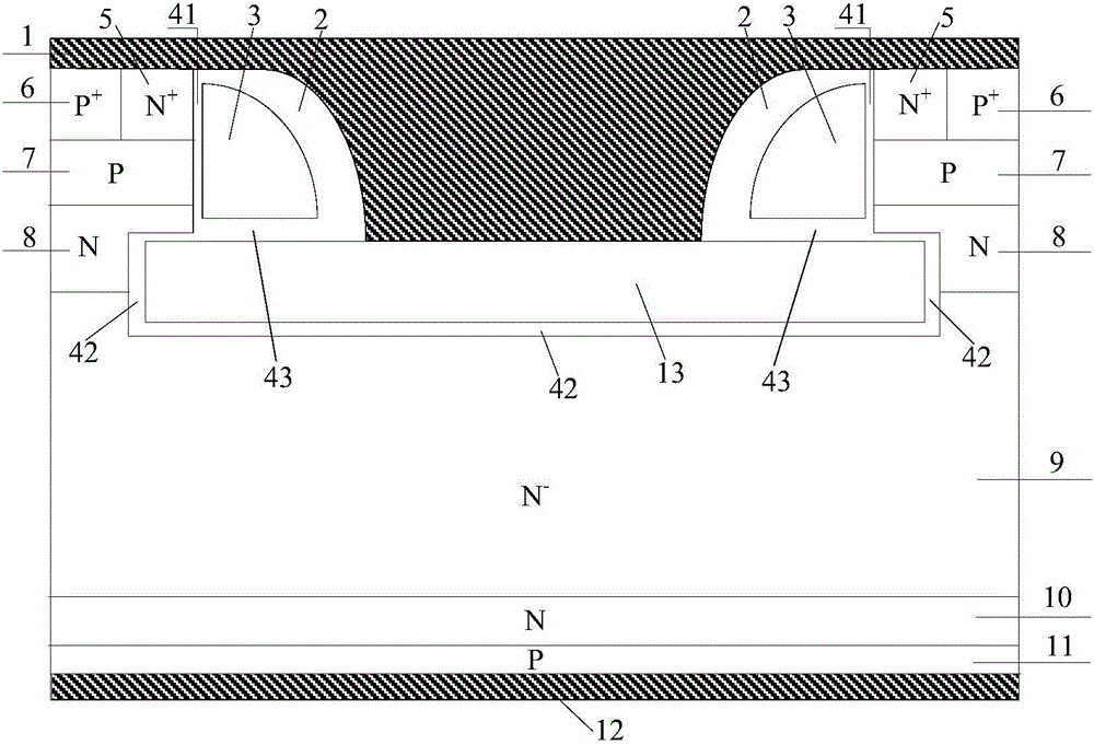
[0044] The trench gate IGBT of this example has a cell structure such as image 3 As shown, on the basis of Embodiment 1, the width of the lower structure of the composite trench structure is greater than the width of the upper structure and extends into the N-type charge storage layer 8; the width of the p-type base region 7 formed is less than In the case of 1 micrometer, the width of the lower structure of the composite trench structure formed is 0.2-0.8 micrometers greater than the width of the upper structure. The underlying structure extending into the N-type charge storage layer 8 further reduces the extraction area of ​​minority carriers, further improves the carrier injection enhancement effect at the emitter end, and can obtain a better device forward voltage drop It is a compromise between switching loss and the N-type charge storage layer's adverse effects on the breakdown voltage of the device, and higher breakdown voltage and reliability of the device are obtained....

Embodiment 3

[0046] The trench gate IGBT of this example has a cell structure such as Figure 4 As shown, on the basis of Example 2, there is also an N+ layer 14 in a part of the region between the lower structure of the composite trench structure and the p-type base region 7, and the concentration of the N+ layer 14 is greater than that of the N-type charge. The concentration of the storage layer 8 and its sidewalls are connected with the composite trench structure; the width of the formed p-type base region 7 is less than 1 micron, and the width of the lower structure of the formed composite trench structure is greater than the width of the upper structure In the case of 0.2 to 0.8 microns, the width of the formed N+ layer 14 is 0.2 to 0.8 microns. The formed N+ layer 14 further reduces the resistance of the region between the lower structure of the composite trench structure and the p-type body region 7, further improves the carrier injection enhancement effect of the emitter terminal, an...


PUM


Abstract

The present invention relates to a trench gate IGBT device and a manufacturing method thereof, and belongs to the power semiconductor device technology field, and relates to an insulated gate bipolar transistor. According to the present invention, by introducing a composite trench structure and a carrier storage layer which are coupled mutually, and introducing an electrode connected with an emitter at the bottom of a gate electrode of an injection enhanced gate transistor (IEGT) device, on one hand, the depth and width of the gate electrode are reduced under a certain trench depth and width, on the other hand, by the shielding effect of the introduced electrode connected with the emitter, the gate capacitance, especially the gate-collector capacitance of the device is reduced, the switching speed of the device is improved, the switching loss of the device is reduced. Meanwhile, by introducing the coupled carrier storage layer, the adverse effect to the positive conduction characteristic of the device which is caused by introducing the gate electrode connected with the emitter is compensated, further the carrier concentration distribution of a whole drift region is improved, and the better compromise of the device positive conduction voltage drop and the switching loss is obtained.

Description

Technical field [0001] The invention belongs to the technical field of power semiconductor devices, and relates to an insulated gate bipolar transistor (IGBT), and in particular to an injection-enhanced trench gate insulated gate bipolar transistor (Injection-Enhanced Gate Transistor, IEGT). Background technique [0002] Insulated gate bipolar transistor (IGBT) is a new type of power electronic device that combines MOS field effect and bipolar transistor. It not only has the advantages of MOSFET easy drive and simple control, but also has the advantages of reduced power transistor conduction voltage, large on-state current, and low loss. It has become one of the core electronic components in modern power electronic circuits and is widely used in Various fields of the national economy such as communications, energy, transportation, industry, medicine, household appliances, and aerospace. The application of IGBT has played an extremely important role in improving the performance o...

Claims


Application Information

Patent Timeline
Patent Type & Authority Applications(China)
IPC IPC(8): H01L29/739H01L21/331
CPCH01L29/66325H01L29/7393H01L2924/13055
Inventor 张金平田丰境底聪刘竞秀李泽宏任敏张波
Owner UNIV OF ELECTRONICS SCI & TECH OF CHINA
Why Eureka
Try Eureka