

Asymmetrical electrode two-dimensional material/graphene heterojunction cascaded photodetector and manufacturing method thereof
A technology of asymmetric electrodes and photodetectors, which is applied in the direction of circuits, electrical components, semiconductor devices, etc., can solve the problems that two-dimensional material detectors cannot meet the requirements, the carrier mobility is small, and the light absorption efficiency is low. Effects of reduced device size, fast response time, and increased photoresponse
- Summary
- Abstract
- Description
- Claims
- Application Information
AI Technical Summary
Problems solved by technology
Method used
Image

Examples
Embodiment 1
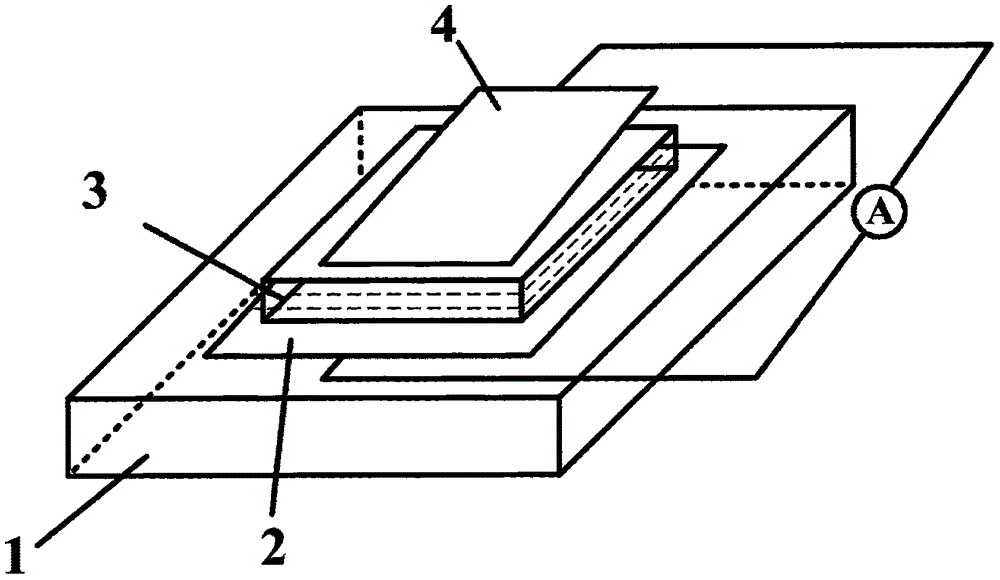
[0030] S11. Growth of single-layer graphene and MoS by CVD 2 and other two-dimensional materials.
[0031] S12, by thermal evaporation on Si / SiO 2 A 40 nm thick Au electrode (first electrode) was prepared on the surface.
[0032] S13. After doping the obtained graphene and the two-dimensional material to different degrees, use PMMA to transfer the graphene and the two-dimensional material to the metal electrode (the surface of the first electrode), respectively, to obtain the two-dimensional material / graphene / two-dimensional material double heterojunction;
[0033] S14. Patterning the obtained two-dimensional material / graphene / two-dimensional material double heterojunction by photolithography;
[0034] S15. Evaporate 20nm Ag on the two-dimensional material / graphene / two-dimensional material double heterojunction by thermal evaporation as the second electrode to obtain a two-dimensional material / graphene / two-dimensional material double heterojunction photodetector.
Embodiment 2
[0036] S21. Growth of single-layer graphene and MoS by CVD 2 and other two-dimensional materials.
[0037] S22, by thermal evaporation on Si / SiO 2 A 40 nm thick Au electrode (first electrode) was prepared on the surface.
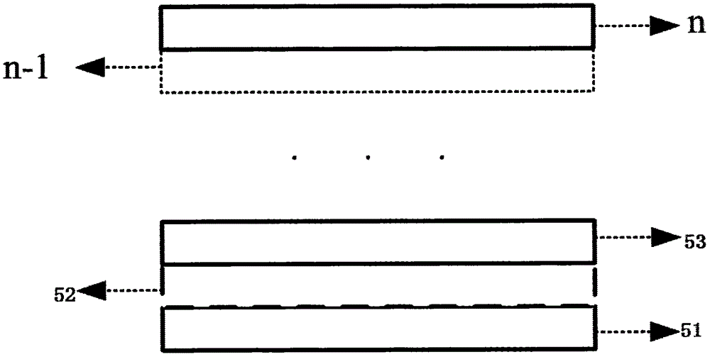
[0038] S23. After doping the obtained graphene and the two-dimensional material to different degrees, use PMMA to transfer the graphene and the two-dimensional material to the metal electrode (the surface of the first electrode), respectively, to obtain graphene / two-dimensional material / graphene / Two-dimensional materials / graphene four heterojunctions;
[0039] S24. Patterning the obtained graphene / two-dimensional material / graphene / two-dimensional material / graphene four heterojunctions by photolithography;
[0040] S25. Use thermal evaporation to evaporate 20nm Ag on the double heterojunction of two-dimensional material / graphene / two-dimensional material as the second electrode, and obtain four heterojunctions of graphene / two-dimensional material / graphene / ...
Embodiment 3
[0042] S31. Growth of single-layer graphene and MoS by CVD 2 and other two-dimensional materials.
[0043] S32, by thermal evaporation on Si / SiO 2 A 40 nm thick Au electrode (first electrode) was prepared on the surface.
[0044] S33. After doping the obtained graphene and the two-dimensional material to different degrees, transfer the graphene and the two-dimensional material to the metal electrode (the surface of the first electrode) respectively using PMMA to obtain the graphene / two-dimensional material 1 (MoS 2 ) / graphene / two-dimensional materials 2 (WS 2 ) / graphene and other two-dimensional materials combined with graphene to form a heterojunction;
[0045] S34, the obtained graphene / two-dimensional material 1 (MoS 2 ) / graphene / two-dimensional materials 2 (WS 2 ) / graphene and other two-dimensional materials combined with graphene to form a heterojunction for patterning;
[0046]S35. Using thermal evaporation to vapor-deposit 20nmAg on the double heterojunction of tw...
PUM
| Property | Measurement | Unit |
|---|---|---|
| thickness | aaaaa | aaaaa |
Abstract
Description
Claims
Application Information