Device and method used for overlay error measurement
An overlay error and overlay mark technology, which is applied in the field of lithography, can solve problems such as the inability to obtain overlay signals, the inability to collect evanescent waves, and the large size of overlay marks, so as to meet the requirements of measurement accuracy and the effective exposure area Small, cost-reducing effect
- Summary
- Abstract
- Description
- Claims
- Application Information
AI Technical Summary
Problems solved by technology
Method used
Image
Examples
Embodiment 1
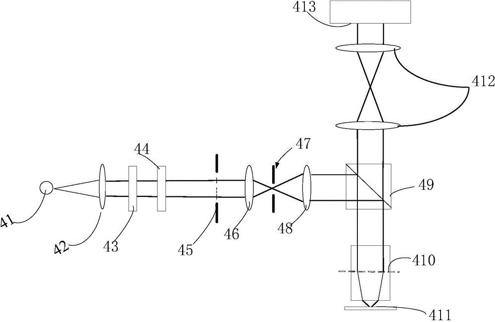
[0040] Such as figure 2 As shown, the device for overlay error detection of this embodiment includes the following components:
[0041] The light source 41 is used to generate measurement light. Specifically, the light source 41 may be a white light source, a broadband light source or a composite light source composed of several discrete spectral lines. Among them, the white light source can use Xe light source, etc.; the broadband refers to the generation of light including ultraviolet, visible and infrared bands or the combination of the above bands; the composite light source can be obtained by mixing several lasers with different wavelengths.
[0042] The illumination system is used to inject measurement light into the objective lens 410 . Specifically, the illumination system sequentially includes along the direction of light propagation: a collimating beam mirror 42 for collimating the measuring light, a filter 43 for generating monochromatic light, a polarizer 44 for...
Embodiment 2
[0067] Such as Figure 11 As shown, in this embodiment, the polarizer 44 is removed on the basis of embodiment 1, and the remaining parts are the same, that is, the polarizer is not necessarily necessary, and the difference between the above two different aperture stops 45 can be obtained in the case of no polarizer. Overlay signal, and then calculate the overlay error.
[0068] Compared with the prior art, the present invention has the following advantages:
[0069] 1. The present invention uses the position information of diffracted light to measure the overlay error, and the measurement signal is not affected by the uniformity of illumination, uniformity of transmittance, etc.;
[0070] 2. The size of the measurement mark is smaller and the effective exposure area occupied is smaller, thereby reducing the cost of overlay marking and the impact on chip manufacturing;
[0071] 3. Due to the use of small-sized measurement marks, the present invention can be distinguished fro...
PUM
| Property | Measurement | Unit |
|---|---|---|
| size | aaaaa | aaaaa |
Abstract
Description
Claims
Application Information


